AD9268
Common-Mode Voltage Servo
typically at very low levels and do not limit SFDR when the
ADC is quantizing large-signal inputs, dithering converts these
tones to noise and produces a whiter noise floor.
In applications where there may be a voltage loss between the VCM
output of the AD9268 and the analog inputs, the common-mode
voltage servo can be enabled. When the inputs are ac-coupled and
a resistance of >100 Ω is placed between the VCM output and the
analog inputs, a significant voltage drop can occur and the
common-mode voltage servo should be enabled. Setting Bit 0 in
Register 0x0F to a logic high enables the VCM servo mode. In
this mode, the AD9268 monitors the common-mode input level
at the analog inputs and adjusts the VCM output level to keep the
common-mode input voltage at an optimal level. If both channels
are operational, Channel A is monitored. However, if Channel A
is in power-down or standby mode, then the Channel B input is
monitored.
Small-Signal FFT
For small-signal inputs, the front-end sampling circuit typically
contributes very little distortion, and, therefore, the SFDR is likely
to be limited by tones caused by DNL errors due to random com-
ponent mismatches. Therefore, for small-signal inputs (typically,
those below −6 dBFS), dithering can significantly improve
SFDR by converting these DNL tones to white noise.
Static Linearity
Dithering also removes sharp local discontinuities in the INL
transfer function of the ADC and reduces the overall peak-to-
peak INL.
Dither
In receiver applications, utilizing dither helps to reduce DNL errors
that cause small-signal gain errors. Often this issue is overcome
by setting the input noise 5 dB to 10 dB above the converter
noise. By utilizing dither within the converter to correct the
DNL errors, the input noise requirement can be reduced.
The AD9268 has an optional dither mode that can be selected
for one or both channels. Dithering is the act of injecting a known
but random amount of white noise, commonly referred to as
dither, into the input of the ADC. Dithering has the effect of
improving the local linearity at various points along the ADC
transfer function. Dithering can significantly improve the SFDR
when quantizing small-signal inputs, typically when the input
level is below −6 dBFS.
Differential Input Configurations
Optimum performance is achieved while driving the AD9268
in a differential input configuration. For baseband applications,
the AD8138, ADA4937-2, and ADA4938-2 differential drivers
provide excellent performance and a flexible interface to the
ADC.
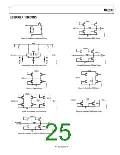
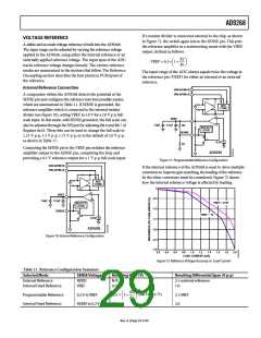
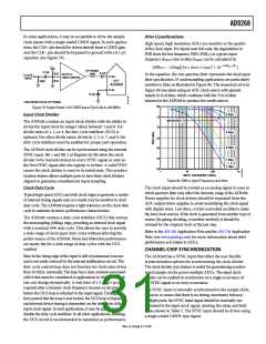
As shown in Figure 65, the dither that is added to the input of
the ADC through the dither DAC is precisely subtracted out
digitally to minimize SNR degradation. When dithering is
enabled, the dither DAC is driven by a pseudorandom number
generator (PN gen). In the AD9268, the dither DAC is precisely
calibrated to result in only a very small degradation in SNR and
SINAD. The typical SNR and SINAD degradation values, with
dithering enabled, are only 1 dB and 0.8 dB, respectively.
The output common-mode voltage of the ADA4938-2 is easily
set with the VCM pin of the AD9268 (see Figure 66), and the
driver can be configured in a Sallen-Key filter topology to
provide band limiting of the input signal.
15pF
200Ω
AD9268
33Ω
5pF
15Ω
VIN
90Ω
DOUT
ADC CORE
VIN–
VIN+
AVDD
76.8Ω
VIN
AD9268
ADA4938-2
0.1µF
DITHER
DAC
33Ω
15Ω
VCM
120Ω
15pF
200Ω
PN GEN
DITHER ENABLE
Figure 66. Differential Input Configuration Using the ADA4938-2
Figure 65. Dither Block Diagram
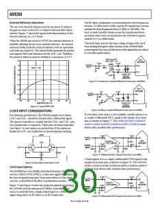
For baseband applications in which SNR is a key parameter,
differential transformer coupling is the recommended input
configuration. An example is shown in Figure 67. To bias the
analog input, the VCM voltage can be connected to the center
tap of the secondary winding of the transformer.
Large-Signal FFT
In most cases, dithering does not improve SFDR for large-signal
inputs close to full scale, for example, with a −1 dBFS input. For
large-signal inputs, the SFDR is typically limited by front-end
sampling distortion, which dithering cannot improve. However,
even for such large-signal inputs, dithering may be useful for
certain applications because it makes the noise floor whiter.
As is common in pipeline ADCs, the AD9268 contains small
DNL errors caused by random component mismatches that
produce spurs or tones that make the noise floor somewhat
randomly colored part-to-part. Although these tones are
C2
R2
VIN+
R1
2V p-p
49.9Ω
C1
R1
AD9268
R2
VCM
VIN–
0.1µF
C2
Figure 67. Differential Transformer-Coupled Configuration
Rev. A | Page 2ꢁ of 44

 ADI [ ADI ]