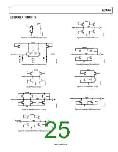
AD9268
If a resistor divider is connected external to the chip, as shown
in Figure 71, the switch again sets to the SENSE pin. This puts
the reference amplifier in a noninverting mode with the VREF
output, defined as follows:
VOLTAGE REFERENCE
A stable and accurate voltage reference is built into the AD9268.
The input range can be adjusted by varying the reference voltage
applied to the AD9268, using either the internal reference or an
externally applied reference voltage. The input span of the ADC
tracks reference voltage changes linearly. The various reference
modes are summarized in the sections that follow. The Reference
Decoupling section describes the best practices PCB layout of
the reference.
R2
R1
⎛
⎝
⎞
⎟
⎠
VREF = 0.5× 1+
⎜
The input range of the ADC always equals twice the voltage at
the reference pin (VREF) for either an internal or an external
reference.
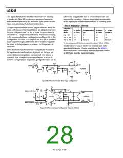
Internal Reference Connection
VIN+A/VIN+B
VIN–A/VIN–B
A comparator within the AD9268 detects the potential at the
SENSE pin and configures the reference into four possible modes,
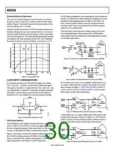
which are summarized in Table 11. If SENSE is grounded, the
reference amplifier switch is connected to the internal resistor
divider (see Figure 70), setting VREF to 1.0 V for a 2.0 V p-p full-
scale input. In this mode, with SENSE grounded, the full scale can
also be adjusted through the SPI port by adjusting Bit 6 and Bit 7 of
Register 0x18. These bits can be used to change the full scale to
1.25 V p-p, 1.5 V p-p, 1.75 V p-p, or to the default of 2.0 V p-p,
as shown in Table 17.
ADC
CORE
VREF
1.0µF
0.1µF
R2
SELECT
LOGIC
SENSE
0.5V
R1
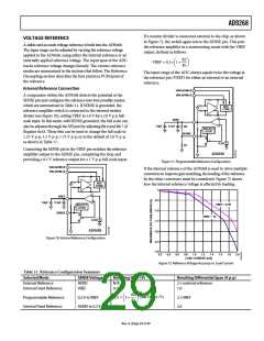
Connecting the SENSE pin to the VREF pin switches the reference
amplifier output to the SENSE pin, completing the loop and
providing a 0.5 V reference output for a 1 V p-p full-scale input.
AD9268
Figure 71. Programmable Reference Configuration
VIN+A/VIN+B
VIN–A/VIN–B
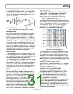
If the internal reference of the AD9268 is used to drive multiple
converters to improve gain matching, the loading of the reference
by the other converters must be considered. Figure 72 shows
how the internal reference voltage is affected by loading.
0
ADC
CORE
VREF
–0.5
1.0µF
0.1µF
VREF = 0.5V
SELECT
LOGIC
–1.0
SENSE
VREF = 1V
0.5V
–1.5
AD9268
–2.0
Figure 70. Internal Reference Configuration
–2.5
–3.0
0.2
0.4
0.6
0.8
1.0
1.2
1.4
1.6
1.8
2.0
LOAD CURRENT (mA)
Figure 72. Reference Voltage Accuracy vs. Load Current
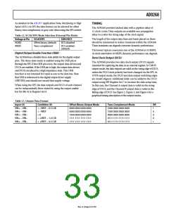
Table 11. Reference Configuration Summary
Selected Mode
SENSE Voltage
Resulting VREF (V)
Resulting Differential Span (V p-p)
External Reference
Internal Fixed Reference
AVDD
VREF
N/A
±.ꢀ
2 × external reference
1.±
R2
R1
⎛
⎞
⎟
(see Figure ꢁ1)
±.ꢀ × 1+
Programmable Reference
Internal Fixed Reference
±.2 V to VREF
AGND to ±.2 V
2 × VREF
2.±
⎜
⎝
⎠
1.±
Rev. A | Page 29 of 44

 ADI [ ADI ]