AD9268
As detailed in the AN-877 Application Note, Interfacing to High
Speed ADCs via SPI, the data format can be selected for offset
binary, twos complement, or gray code when using the SPI control.
TIMING
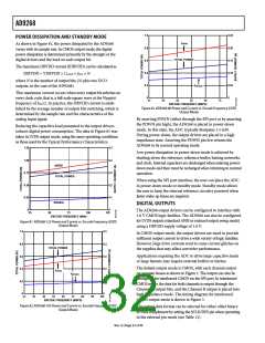
The AD9268 provides latched data with a pipeline delay of
12 clock cycles. Data outputs are available one propagation
delay (tPD) after the rising edge of the clock signal.
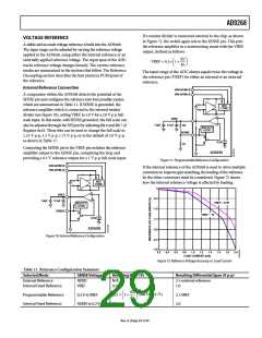
Table 12. SCLK/DFS Mode Selection (External Pin Mode)
The length of the output data lines and loads placed on them
should be minimized to reduce transients within the AD9268.
These transients can degrade converter dynamic performance.
Voltage at Pin
SCLK/DFS
SDIO/DCS
AGND
AVDD
Offset binary (default)
Twos complement
DCS disabled
DCS enabled
(default)
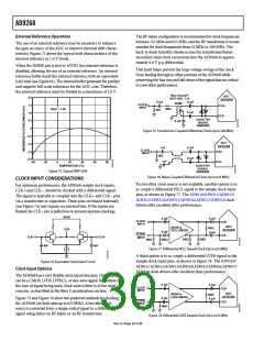
The lowest typical conversion rate of the AD9268 is 10 MSPS.
At clock rates below 10 MSPS, dynamic performance can degrade.
Digital Output Enable Function (OEB)
The AD9268 has a flexible three-state ability for the digital output
pins. The three-state mode is enabled using the OEB pin or
through the SPI. If the OEB pin is low, the output data drivers and
DCOs are enabled. If the OEB pin is high, the output data drivers
and DCOs are placed in a high impedance state. This OEB
function is not intended for rapid access to the data bus. Note
that OEB is referenced to the digital output driver supply
(DRVDD) and should not exceed that supply voltage.
Data Clock Output (DCO)
The AD9268 provides two data clock output (DCO) signals
intended for capturing the data in an external register. In CMOS
output mode, the data outputs are valid on the rising edge of DCO,
unless the DCO clock polarity has been changed via the SPI. In
LVDS output mode, the DCO and data output switching edges
are closely aligned. Additional delay can be added to the DCO
output using SPI Register 0x17 to increase the data setup time.
In this case, the Channel A output data is valid on the rising
edge of DCO, and the Channel B output data is valid on the
falling edge of DCO. See Figure 2, Figure 3, and Figure 4 for a
graphical timing description of the output modes.
When using the SPI, the data outputs and DCO of each channel
can be independently three-stated by using the output enable
bar bit (Bit 4) in Register 0x14.
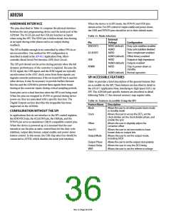
Table 13. Output Data Format
Input (V)
Condition (V)
< −VREF − ±.ꢀ LSB
= −VREF
Offset Binary Output Mode
±±±± ±±±± ±±±± ±±±±
±±±± ±±±± ±±±± ±±±±
1±±± ±±±± ±±±± ±±±±
1111 1111 1111 1111
1111 1111 1111 1111
Twos Complement Mode
1±±± ±±±± ±±±± ±±±±
1±±± ±±±± ±±±± ±±±±
±±±± ±±±± ±±±± ±±±±
±111 1111 1111 1111
±111 1111 1111 1111
OR
1
±
±
±
VIN+ − VIN−
VIN+ − VIN−
VIN+ − VIN−
VIN+ − VIN−
VIN+ − VIN−
= ±
= +VREF − 1.± LSB
> +VREF − ±.ꢀ LSB
1
Rev. A | Page 33 of 44

 ADI [ ADI ]