AD9268
1.0
0.25
POWER DISSIPATION AND STANDBY MODE
I
AVDD
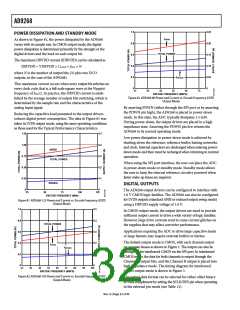
As shown in Figure 81, the power dissipated by the AD9268
varies with its sample rate. In CMOS output mode, the digital
power dissipation is determined primarily by the strength of the
digital drivers and the load on each output bit.
0.8
0.6
0.4
0.2
0
0.20
0.15
0.10
0.05
0
TOTAL POWER
The maximum DRVDD current (IDRVDD) can be calculated as
IDRVDD = VDRVDD × CLOAD × fCLK × N
where N is the number of output bits (32 plus two DCO
outputs, in the case of the AD9268).
I
DRVDD
This maximum current occurs when every output bit switches on
every clock cycle, that is, a full-scale square wave at the Nyquist
frequency of fCLK/2. In practice, the DRVDD current is estab-
lished by the average number of output bits switching, which is
determined by the sample rate and the characteristics of the
analog input signal.
25
35
45
55
65
75
ENCODE FREQUENCY (MSPS)
Figure 83. AD9268-80 Power and Current vs. Encode Frequency (LVDS
Output Mode)
By asserting PDWN (either through the SPI port or by asserting
the PDWN pin high), the AD9268 is placed in power-down
mode. In this state, the ADC typically dissipates 3.3 mW.
During power-down, the output drivers are placed in a high
impedance state. Asserting the PDWN pin low returns the
AD9268 to its normal operating mode.
Reducing the capacitive load presented to the output drivers
reduces digital power consumption. The data in Figure 81 was
taken in LVDS output mode, using the same operating conditions
as those used for the Typical Performance Characteristics.
1.25
0.5
Low power dissipation in power-down mode is achieved by
shutting down the reference, reference buffer, biasing networks,
and clock. Internal capacitors are discharged when entering power-
down mode and then must be recharged when returning to normal
operation.
1.00
0.75
0.50
0.25
0
0.4
0.3
0.2
0.1
0
IAVDD
TOTAL POWER
When using the SPI port interface, the user can place the ADC
in power-down mode or standby mode. Standby mode allows
the user to keep the internal reference circuitry powered when
faster wake-up times are required.
IDRVDD
DIGITAL OUTPUTS
The AD9268 output drivers can be configured to interface with
1.8 V CMOS logic families. The AD9268 can also be configured
for LVDS outputs (standard ANSI or reduced output swing mode)
using a DRVDD supply voltage of 1.8 V.
25
50
75
100
125
ENCODE FREQUENCY (MHz)
Figure 81. AD9268-125 Power and Current vs. Encode Frequency (LVDS
Output Mode)
1.0
0.5
In CMOS output mode, the output drivers are sized to provide
sufficient output current to drive a wide variety of logic families.
However, large drive currents tend to cause current glitches on
the supplies that may affect converter performance.
0.8
0.6
0.4
0.2
0
0.4
0.3
0.2
0.1
0
TOTAL POWER
Applications requiring the ADC to drive large capacitive loads
or large fanouts may require external buffers or latches.
The default output mode is CMOS, with each channel output
on separate busses as shown in Figure 2. The output can also be
configured for interleaved CMOS via the SPI port. In interleaved
CMOS mode, the data for both channels is output through the
Channel A output bits, and the Channel B output is placed into
high impedance mode. The timing diagram for interleaved
CMOS output mode is shown in Figure 3.
I
AVDD
I
DRVDD
25
35
45
55
65
75
85
95
105
ENCODE FREQUENCY (MSPS)
Figure 82. AD9268-105 Power and Current vs. Encode Frequency (LVDS
Output Mode)
The output data format can be selected for either offset binary
or twos complement by setting the SCLK/DFS pin when operating
in the external pin mode (see Table 12).
Rev. A | Page 32 of 44

 ADI [ ADI ]