AD9268
The signal characteristics must be considered when selecting
a transformer. Most RF transformers saturate at frequencies
below a few megahertz (MHz). Excessive signal power can also
cause core saturation, which leads to distortion.
achieved by using a ferrite bead in series with a resistor and
removing the capacitors. However, these values are dependent
on the input signal and should be used only as a starting guide.
Table 10. Example RC Network
At input frequencies in the second Nyquist zone and above, the
noise performance of most amplifiers is not adequate to achieve
the true SNR performance of the AD9268. For applications in
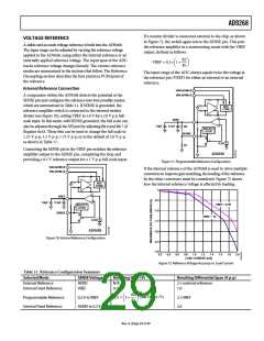
which SNR is a key parameter, differential double balun coupling
is the recommended input configuration (see Figure 68). In this
configuration, the input is ac-coupled, and the CML is provided
to each input through a 33 Ω resistor. These resistors compensate
for losses in the input baluns to provide a 50 Ω impedance to
the driver.
Frequency
Range
(MHz)
R1 Series C1 Differential R2 Series C2 Shunt
(Ω Each) (pF)
(Ω Each)
(pF Each)
± to 1±±
1±± to 2±± 1±
1±± to 3±± 1±1
33
ꢀ
ꢀ
1ꢀ
1±
66
1ꢀ
1±
Remove
Remove
1 In this configuration, R1 is a ferrite bead with a value of 1± Ω @ 1±± MHz.
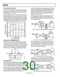
An alternative to using a transformer-coupled input at fre-
quencies in the second Nyquist zone is to use the AD8352
differential driver. An example is shown in Figure 69. See the
AD8352 data sheet for more information.
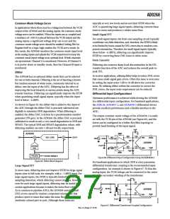
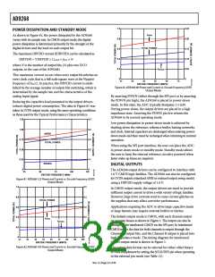
In the double balun and transformer configurations, the value of
the input capacitors and resistors is dependent on the input fre-
quency and source impedance and may need to be reduced or
removed. Table 10 displays recommended values to set the RC
network. At higher input frequencies, good performance can be
C2
0.1µF
0.1µF
R1
R2
R2
VIN+
2V p-p
33Ω
33Ω
P
A
S
S
P
C1
R1
AD9268
0.1µF
0.1µF
VCM
VIN–
C2
Figure 68. Differential Double Balun Input Configuration
V
CC
0.1µF
0Ω
R
0.1µF
16
1
8, 13
11
0.1µF
0.1µF
ANALOG INPUT
R
R
VIN+
2
200Ω
C
AD9268
AD8352
10
R
G
C
D
D
3
4
5
200Ω
VCM
VIN–
14
0.1µF
ANALOG INPUT
0Ω
0.1µF
0.1µF
Figure 69. Differential Input Configuration Using the AD8352
Rev. A | Page 28 of 44

 ADI [ ADI ]