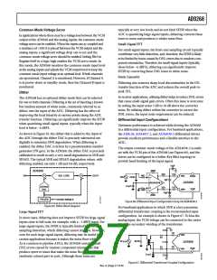
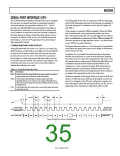
AD9268
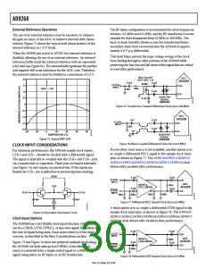
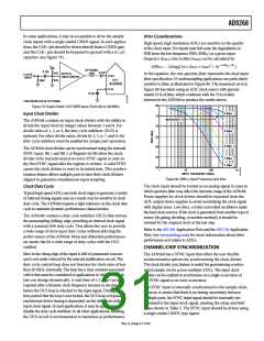
In some applications, it may be acceptable to drive the sample
clock inputs with a single-ended CMOS signal. In such applica-
tions, the CLK+ pin should be driven directly from a CMOS gate,
and the CLK− pin should be bypassed to ground with a 0.1 ꢀF
capacitor (see Figure 79).
Jitter Considerations
High speed, high resolution ADCs are sensitive to the quality
of the clock input. For inputs near full scale, the degradation in
SNR from the low frequency SNR (SNRLF) at a given input
frequency (fINPUT) due to jitter (tJRMS) can be calculated by
SNRHF = −10 log[(2π × fINPUT × tJRMS)2 + 10 (−SNR /10)
]
LF
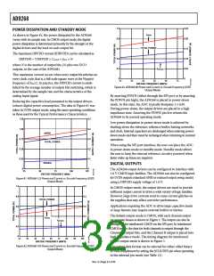
V
CC
OPTIONAL
100Ω
0.1µF
1
0.1µF
1kΩ
1kΩ
AD951x
CMOS DRIVER
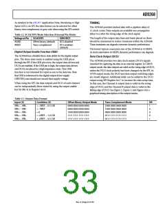
In the equation, the rms aperture jitter represents the clock input
jitter specification. IF undersampling applications are particularly
sensitive to jitter, as illustrated in Figure 80. The measured curve in
Figure 80 was taken using an ADC clock source with approxi-
mately 65 fs of jitter, which combines with the 70 fs of jitter
inherent in the AD9268 to produce the results shown.
80
CLOCK
INPUT
CLK+
ADC
AD9268
50Ω
CLK–
0.1µF
1
50Ω RESISTOR IS OPTIONAL.
Figure 79. Single-Ended 1.8 V CMOS Input Clock (Up to 200 MHz)
0.05ps
Input Clock Divider
75
MEASURED
The AD9268 contains an input clock divider with the ability to
divide the input clock by integer values between 1 and 8. For
divide ratios of 1, 2, or 4, the duty cycle stabilizer (DCS) is
optional. For other divide ratios, divide by 3, 5, 6, 7, and 8, the
duty cycle stabilizer must be enabled for proper part operation.
70
0.20ps
65
0.50ps
60
55
50
The AD9268 clock divider can be synchronized using the external
SYNC input. Bit 1 and Bit 2 of Register 0x100 allow the clock
divider to be resynchronized on every SYNC signal or only on
the first SYNC signal after the register is written. A valid SYNC
causes the clock divider to reset to its initial state. This synchro-
nization feature allows multiple parts to have their clock dividers
aligned to guarantee simultaneous input sampling.
1.00ps
1.50ps
1
10
100
1k
INPUT FREQUENCY (MHz)
Figure 80. SNR vs. Input Frequency and Jitter
The clock input should be treated as an analog signal in cases in
which aperture jitter may affect the dynamic range of the AD9268.
Power supplies for clock drivers should be separated from the
ADC output driver supplies to avoid modulating the clock signal
with digital noise. Low jitter, crystal-controlled oscillators make
the best clock sources. If the clock is generated from another type of
source (by gating, dividing, or another method), it should be
retimed by the original clock at the last step.
Clock Duty Cycle
Typical high speed ADCs use both clock edges to generate a variety
of internal timing signals and, as a result, may be sensitive to clock
duty cycle. The AD9268 requires a tight tolerance on the clock duty
cycle to maintain dynamic performance characteristics.
The AD9268 contains a duty cycle stabilizer (DCS) that retimes
the nonsampling (falling) edge, providing an internal clock signal
with a nominal 50% duty cycle. This allows the user to provide
a wide range of clock input duty cycles without affecting the
perfor-mance of the AD9268. Noise and distortion performance
are nearly flat for a wide range of duty cycles with the DCS
enabled.
Refer to the AN-501 Application Note and the AN-756 Application
Note (see www.analog.com) for more information about jitter
performance as it relates to ADCs.
CHANNEL/CHIP SYNCHRONIZATION
Jitter in the rising edge of the input is still of paramount concern
and is not easily reduced by the internal stabilization circuit. The
duty cycle control loop does not function for clock rates of less
than 20 MHz, nominally. The loop has a time constant associated
with it that must be considered in applications in which the clock
rate can change dynamically. A wait time of 1.5 μs to 5 μs is
required after a dynamic clock frequency increase or decrease
before the DCS loop is relocked to the input signal. During the
time period that the loop is not locked, the DCS loop is bypassed,
and internal device timing is dependent on the duty cycle of the
input clock signal. In such applications, it may be appropriate to
disable the duty cycle stabilizer. In all other applications, enabling
the DCS circuit is recommended to maximize ac performance.
The AD9268 has a SYNC input that offers the user flexible
synchronization options for synchronizing the clock divider.
The clock divider sync feature is useful for guaranteeing synchro-
nized sample clocks across multiple ADCs. The input clock
divider can be enabled to synchronize on a single occurrence of
the SYNC signal or on every occurrence.
The SYNC input is internally synchronized to the sample clock;
however, to ensure that there is no timing uncertainty between
multiple parts, the SYNC input signal should be externally syn-
chronized to the input clock signal, meeting the setup and hold
times shown in Table 5. The SYNC input should be driven using
a single-ended CMOS-type signal.
Rev. A | Page 31 of 44

 ADI [ ADI ]