AD9228
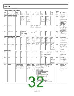
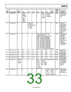
Default
Value
(Hex)
Addr.
(Hex)
Bit 7
Bit 0
(LSB)
Default Notes/
Comments
Parameter Name (MSB)
Bit 6
Bit 5
Bit 4
Bit 3
Bit 2
Bit 1
1ꢁ
output_mode
X
0 = LVDS
ANSI
(default)
1 = LVDS
low
X
X
X
Output
invert
1 = on
0 = off
(default)
00 = offset binary
(default)
01 = twos
0x00
Configures the
outputs and the
format of the
data.
complement
power,
(IEEE
159ꢃ.3
similar)
15
output_adjust
X
X
Output driver
termination
00 = none (default)
01 = 200 Ω
10 = 100 Ω
11 = 100 Ω
X
X
X
X
0x00
Determines
LVDS or other
output properties.
Primarily func-
tions to set the
LVDS span and
common-mode
levels in place of
an external
resistor.
1ꢃ
output_phase
X
X
X
X
0011 = output clock phase adjust
(0000 through 1010)
0x03
On devices that
utilize global
clock divide,
determines
which phase of
the divider
output is used to
supply the
output clock.
Internal latching
is unaffected.
(Default: 1ꢀ0° relative to DATA edge)
0000 = 0° relative to DATA edge
0001 = ꢃ0° relative to DATA edge
0010 = 120° relative to DATA edge
0011 = 1ꢀ0° relative to DATA edge
0100 = 2ꢁ0° relative to DATA edge
0101 = 300° relative to DATA edge
0110 = 3ꢃ0° relative to DATA edge
0111 = ꢁ20° relative to DATA edge
1000 = ꢁꢀ0° relative to DATA edge
1001 = 5ꢁ0° relative to DATA edge
1010 = ꢃ00° relative to DATA edge
1011 to 1111 = ꢃꢃ0° relative to DATA edge
19
1A
1B
1C
21
user_patt1_lsb
user_patt1_msb
user_patt2_lsb
user_patt2_msb
serial_control
Bꢂ
Bꢃ
B1ꢁ
Bꢃ
B5
B13
B5
Bꢁ
B12
Bꢁ
B3
B2
B1
B9
B1
B9
B0
Bꢀ
B0
Bꢀ
0x00
0x00
0x00
0x00
0x00
User-defined
pattern, 1 LSB.
B15
Bꢂ
B11
B3
B10
B2
User-defined
pattern, 1 MSB.
User-defined
pattern, 2 LSB.
B15
B1ꢁ
X
B13
X
B12
X
B11
B10
User-defined
pattern, 2 MSB.
LSB first
1 = on
0 = off
<10
MSPS,
low
encode
rate
000 = 12 bits (default, normal bit
stream)
001 = ꢀ bits
010 = 10 bits
011 = 12 bits
Serial stream
control. Default
causes MSB first
and the native
bit stream
(default)
mode
1 = on
0 = off
(default)
100 = 1ꢁ bits
(global).
22
serial_ch_stat
X
X
X
X
X
X
Channel
output
reset
Channel
power-
down
0x00
Used to power
down individual
sections of a
1 = on
0 = off
1 = on
0 = off
converter (local).
(default) (default)
Rev. 0 | Page 33 of 52

 ADI [ ADI ]