AD9228
MEMORY MAP
READING THE MEMORY MAP TABLE
RESERVED LOCATIONS
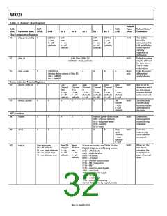
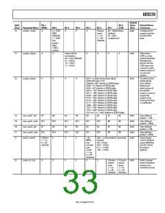
Each row in the memory map table has eight address locations.
The memory map is roughly divided into three sections: chip
configuration register map (Address 0x00 to Address 0x02), device
index and transfer register map (Address 0x05 and Address 0xFF),
and program register map (Address 0x08 to Address 0x25).
Undefined memory locations should not be written to except
when writing the default values suggested in this data sheet.
Addresses that have values marked as 0 should be considered
reserved and have a 0 written into their registers during power-up.
DEFAULT VALUES
The left-hand column of the memory map indicates the register
address number in hexadecimal. The default value of this address is
shown in hexadecimal in the right-hand column. The Bit 7 (MSB)
column is the start of the default hexadecimal value given. For
example, Hexadecimal Address 0x09, Clock, has a hexadecimal
default value of 0x01. This means Bit 7 = 0, Bit 6 = 0, Bit 5 = 0,
Bit 4 = 0, Bit 3 = 0, Bit 2 = 0, Bit 1 = 0, and Bit 0 = 1, or 0000 0001
in binary. This setting is the default for the duty cycle stabilizer in
the on condition. By writing a 0 to Bit 6 at this address, the duty
cycle stabilizer turns off. For more information on this and other
functions, consult the user manual Interfacing to High Speed
ADCs via SPI.
Coming out of reset, critical registers are preloaded with default
values. These values are indicated in Table 15, where an X refers
to an undefined feature.
LOGIC LEVELS
An explanation of various registers follows: “Bit is set” is
synonymous with “bit is set to Logic 1” or “writing Logic 1 for
the bit.” Similarly, “clear a bit” is synonymous with “bit is set to
Logic 0” or “writing Logic 0 for the bit.”
Rev. 0 | Page 31 of 52

 ADI [ ADI ]