AD9228
EVALUATION BOARD
each section. At least one 1.8 V supply is needed with a 1 A current
capability for AVDD_DUT and DRVDD_DUT; however, it is
recommended that separate supplies be used for both analog
and digital. To operate the evaluation board using the VGA
option, a separate 5.0 V analog supply is needed. The 5.0 V
supply, or AVDD_5 V, should have a 1 A current capability. To
operate the evaluation board using the SPI and alternate clock
options, a separate 3.3 V analog supply is needed in addition to
the other supplies. The 3.3 V supply, or AVDD_3.3 V, should
have a 1 A current capability as well.
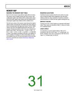
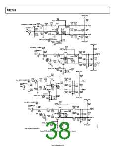
The AD9228 evaluation board provides all of the support cir-
cuitry required to operate the ADC in its various modes and
configurations. The converter can be driven differentially through a
transformer (default) or through the AD8332 driver. The ADC
can also be driven in a single-ended fashion. Separate power pins
are provided to isolate the DUT from the AD8332 drive circuitry.
Each input configuration can be selected by proper connection
of various jumpers (see Figure 72 to Figure 76). Figure 70 shows
the typical bench characterization setup used to evaluate the ac
performance of the AD9228. It is critical that the signal sources
used for the analog input and clock have very low phase noise
(<1 ps rms jitter) to realize the optimum performance of the
converter. Proper filtering of the analog input signal to remove
harmonics and lower the integrated or broadband noise at the
input is also necessary to achieve the specified noise performance.
INPUT SIGNALS
When connecting the clock and analog source, use clean signal
generators with low phase noise, such as Rohde & Schwarz SMHU
or HP8644 signal generators or the equivalent. Use a 1 m, shielded,
RG-58, 50 Ω coaxial cable for making connections to the evalu-
ation board. Enter the desired frequency and amplitude from the
ADC specifications tables. Typically, most ADI evaluation boards
can accept ~2.8 V p-p or 13 dBm sine wave input for the clock.
When connecting the analog input source, it is recommended
to use a multipole, narrow-band, band-pass filter with 50 Ω
terminations. ADI uses TTE, Allen Avionics, and K&L types of
band-pass filters. The filter should be connected directly to the
evaluation board if possible.
See Figure 72 to Figure 80 for the complete schematics and
layout diagrams that demonstrate the routing and grounding
techniques that should be applied at the system level.
POWER SUPPLIES
This evaluation board comes with a wall-mountable switching
power supply that provides a 6 V, 2 A maximum output. Simply
connect the supply to the rated 100 V ac to 240 V ac wall outlet
at 47 Hz to 63 Hz. The other end is a 2.1 mm inner diameter
jack that connects to the PCB at P503. Once on the PC board,
the 6 V supply is fused and conditioned before connecting to
three low dropout linear regulators that supply the proper bias
to each of the various sections on the board.
OUTPUT SIGNALS
The default setup uses the HSC-ADC-FPGA high speed
deserialization board to deserialize the digital output data and
convert it to parallel CMOS. These two channels interface
directly with the ADI standard dual-channel FIFO data capture
board (HSC-ADC-EVALA-DC). Two of the four channels can
then be evaluated at the same time. For more information on
channel settings on these boards and their optional settings,
visit www.analog.com/FIFO.
When operating the evaluation board in a nondefault condition,
L504 to L507 can be removed to disconnect the switching
power supply. This enables the user to bias each section of the
board individually. Use P501 to connect a different supply for
WALL OUTLET
100V TO 240V AC
47Hz TO 63Hz
6V DC
2A MAX
5.0V
1.8V
1.8V
3.3V
3.3V
1.5V
3.3V
–
+
–
+
–
+
–
+
–
+
–
+
–
+
SWITCHING
POWER
SUPPLY
PC
RUNNING
ADC
ANALYZER
AND SPI
USER
ROHDE & SCHWARZ,
HSC-ADC-FPGA
HIGH SPEED
DESERIALIZATION
HSC-ADC-EVALA-DC
FIFO DATA
SMHU,
2V p-p SIGNAL
SYNTHESIZER
BAND-PASS
FILTER
XFMR
INPUT
CAPTURE
BOARD
AD9228
EVALUATION BOARD
BOARD
CHA–CHD
12-BIT
SERIAL
LVDS
SOFTWARE
2 CH
USB
CONNECTION
ROHDE & SCHWARZ,
SMHU,
12-BIT
PARALLEL
CMOS
CLK
2V p-p SIGNAL
SYNTHESIZER
SPI
SPI
SPI
SPI
Figure 70. Evaluation Board Connection
Rev. 0 | Page 35 of 52

 ADI [ ADI ]