AD9228
SERIAL PORT INTERFACE (SPI)
middle of any byte transfer, the SPI state machine is reset and
the device waits for a new instruction.
The AD9228 serial port interface allows the user to configure
the converter for specific functions or operations through a
structured register space provided inside the ADC. This gives
the user added flexibility and customization depending on the
application. Addresses are accessed via the serial port and can
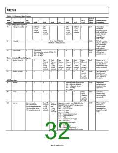
be written to or read from via the port. Memory is organized
into bytes that can be further divided down into fields, as doc-
umented in the Memory Map section. Detailed operational
information can be found in the Analog Devices user manual
Interfacing to High Speed ADCs via SPI.
In addition to the operation modes, the SPI port can be
configured to operate in different manners. For applications
that do not require a control port, the CSB line can be tied and
held high. This places the remainder of the SPI pins in their
secondary mode as defined in the Serial Port Interface (SPI)
section. CSB can also be tied low to enable 2-wire mode. When
CSB is tied low, SCLK and SDIO are the only pins required for
communication. Although the device is synchronized during
power-up, caution must be exercised when using this mode to
ensure that the serial port remains synchronized with the CSB
line. When operating in 2-wire mode, it is recommended to use
a 1-, 2-, or 3-byte transfer exclusively. Without an active CSB
line, streaming mode can be entered but not exited.
There are three pins that define the serial port interface or SPI
to this particular ADC. They are the SCLK, SDIO, and CSB
pins. The SCLK (serial clock) is used to synchronize the read
and write data presented to the ADC. The SDIO (serial data
input/output) is a dual-purpose pin that allows data to be sent
to and read from the internal ADC memory map registers. The
CSB (chip select bar) is an active low control that enables or
disables the read and write cycles (see Table 13).
In addition to word length, the instruction phase determines if
the serial frame is a read or write operation, allowing the serial
port to be used to both program the chip and read the contents
of the on-chip memory. If the instruction is a readback operation,
performing a readback causes the serial data input/output (SDIO)
pin to change direction from an input to an output at the
appropriate point in the serial frame.
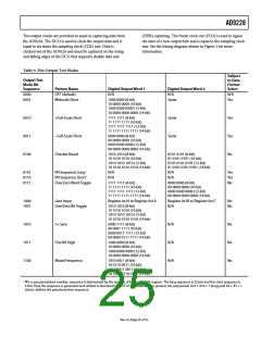
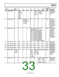
Table 13. Serial Port Pins
Pin
Function
SCLK
Serial Clock. The serial shift clock in. SCLK is used to
synchronize serial interface reads and writes.
Serial Data Input/Output. A dual-purpose pin. The
typical role for this pin is an input or output, depending
on the instruction sent and the relative position in the
timing frame.
SDIO
CSB
Data can be sent in MSB- or LSB-first mode. MSB-first mode
is the default at power-up and can be changed by adjusting the
configuration register. For more information about this and
other features, see the user manual Interfacing to High Speed
ADCs via SPI.
Chip Select Bar (Active Low). This control gates the read
and write cycles.
HARDWARE INTERFACE
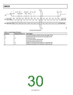
The falling edge of the CSB in conjunction with the rising edge
of the SCLK determines the start of the framing sequence. During
an instruction phase, a 16-bit instruction is transmitted followed
by one or more data bytes, which is determined by Bit Fields
W0 and W1. An example of the serial timing and its definitions
can be found in Figure 68 and Table 14. In normal operation,
CSB is used to signal to the device that SPI commands are to be
received and processed. When CSB is brought low, the device
processes SCLK and SDIO to process instructions. Normally,
CSB remains low until the communication cycle is complete.
However, if connected to a slow device, CSB can be brought
high between bytes, allowing old microcontrollers enough time
to transfer data into shift registers. CSB can be stalled when
transferring one, two, or three bytes of data. When W0 and W1
are set to 11, the device enters streaming mode and continues
to process data, either reading or writing, until the CSB is taken
high to end the communication cycle. This allows complete
memory transfers without having to provide additional instruc-
tions. Regardless of the mode, if CSB is taken high in the
The pins described in Table 13 compose the physical interface
between the user’s programming device and the serial port of
the AD9228. The SCLK and CSB pins function as inputs when
using the SPI interface. The SDIO pin is bidirectional, functioning
as an input during write phases and as an output during readback.
This interface is flexible enough to be controlled by either serial
PROMS or PIC mirocontrollers. This provides the user an
alternative method, other than a full SPI controller, to program
the ADC (see the AN-812 Application Note).
If the user chooses not to use the SPI interface, these pins serve
a dual function and are associated with secondary functions
when the CSB is strapped to AVDD during device power-up.
See the Theory of Operation section for details on which pin-
strappable functions are supported on the SPI pins.
Rev. 0 | Page 29 of 52

 ADI [ ADI ]