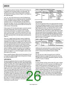
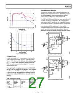
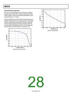
AD9228
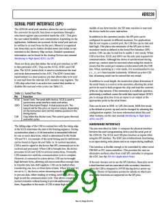
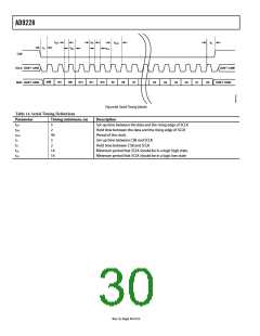
tDS
tHI
tCLK
tH
tS
tDH
tLO
CSB
SCLK DON’T CARE
SDIO DON’T CARE
DON’T CARE
R/W
W1
W0
A12
A11
A10
A9
A8
A7
D5
D4
D3
D2
D1
D0
DON’T CARE
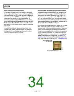
Figure 68. Serial Timing Details
Table 14. Serial Timing Definitions
Parameter
Timing (minimum, ns)
Description
tDS
tDH
tCLK
tS
5
2
ꢁ0
5
Set-up time between the data and the rising edge of SCLK
Hold time between the data and the rising edge of SCLK
Period of the clock
Set-up time between CSB and SCLK
tH
2
Hold time between CSB and SCLK
tHI
tLO
1ꢃ
1ꢃ
Minimum period that SCLK should be in a logic high state
Minimum period that SCLK should be in a logic low state
Rev. 0 | Page 30 of 52

 ADI [ ADI ]