AD9228
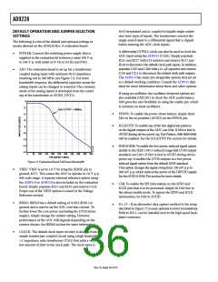
Table 15. Memory Map Register
Default
Value
(Hex)
Addr.
(Hex)
Bit 7
Bit 0
(LSB)
Default Notes/
Comments
Parameter Name (MSB)
Bit 6
Bit 5
Bit 4
Bit 3
Bit 2
Bit 1
Chip Configuration Registers
00
chip_port_config
0
LSB first
1 = on
Soft
reset
1
1
Soft
reset
LSB first
1 = on
0
0x1ꢀ
The nibbles
should be
0 = off
(default)
1 = on
0 = off
(default)
1 = on
0 = off
(default)
0 = off
(default)
mirrored so that
LSB- or MSB-first
mode registers
correctly
regardless of
shift mode.
01
02
chip_id
ꢀ-bit Chip ID Bits ꢂ:0
(AD922ꢀ = 0x02), (default)
0x02
Default is unique
chip ID, different
for each device.
This is a read-
only register.
chip_grade
X
Child ID ꢃ:ꢁ
X
X
X
X
Read
only
Child ID used to
differentiate
graded devices.
(identify device variants of Chip ID)
000 = ꢃ5 MSPS,
001 = ꢁ0 MSPS
Device Index and Transfer Registers
05
device_index_A
X
X
X
Clock
Channel
DCO
1 = on
0 = off
Clock
Channel
FCO
1 = on
0 = off
Data
Channel
D
Data
Channel
C
Data
Channel
B
Data
Channel
A
0x0F
0x00
Bits are set to
determine which
on-chip device
receives the next
write command.
1 = on
1 = on
1 = on
1 = on
(default) (default) (default) (default)
(default) (default) 0 = off
0 = off
0 = off
0 = off
FF
device_update
X
X
X
X
X
X
SW
Synchronously
transfers data
from the master
shift register to
the slave.
transfer
1 = on
0 = off
(default)
ADC Functions
0ꢀ
modes
X
X
X
X
X
X
X
X
X
X
Internal power-down mode
000 = chip run (default)
001 = full power-down
010 = standby
0x00
0x01
Determines
various generic
modes of chip
operation.
011 = reset
09
clock
X
X
Duty
Turns the
cycle
internal duty
cycle stabilizer
on and off.
stabilizer
1 = on
(default)
0 = off
0D
test_io
User test mode
00 = off (default)
01 = on, single alternate 1 = on
10 = on, single once
11 = on, alternate once
Reset PN Reset
long gen PN short
0x00
When set, the
test data is
placed on the
output pins in
place of normal
data.
Output test mode—see Table 9 in the
Digital Outputs and Timing section
0000 = off (default)
0001 = midscale short
0010 = +FS short
0011 = −FS short
gen
0 = off
1 = on
(default) 0 = off
(default)
0100 = checker board output
0101 = PN 23 sequence
0110 = PN 9
0111 = one/zero word toggle
1000 = user input
1001 = one/zero bit toggle
1010 = 1× sync
1011 = one bit high
1100 = mixed bit frequency
(format determined by output_mode)
Rev. 0 | Page 32 of 52

 ADI [ ADI ]