AD9228
Power and Ground Recommendations
Exposed Paddle Thermal Heat Slug Recommendations
When connecting power to the AD9228, it is recommended
that two separate 1.8 V supplies be used: one for analog (AVDD)
and one for digital (DRVDD). If only one supply is available, it
should be routed to the AVDD first and then tapped off and
isolated with a ferrite bead or a filter choke preceded by
decoupling capacitors for the DRVDD. The user can employ
several different decoupling capacitors to cover both high and
low frequencies. These should be located close to the point of
entry at the PC board level and close to the parts with minimal
trace length.
It is required that the exposed paddle on the underside of the
ADC is connected to analog ground (AGND) to achieve the
best electrical and thermal performance of the AD9228. An
exposed continuous copper plane on the PCB should mate to
the AD9228 exposed paddle, Pin 0. The copper plane should
have several vias to achieve the lowest possible resistive thermal
path for heat dissipation to flow through the bottom of the PCB.
These vias should be solder filled or plugged.
To maximize the coverage and adhesion between the ADC and
PCB, partition the continuous copper plane by overlaying a
silkscreen on the PCB into several uniform sections. This provides
several tie points between the two during the reflow process.
Using one continuous plane with no partitions only guarantees
one tie point between the ADC and PCB. See Figure 69 for a
PCB layout example. For detailed information on packaging
and the PCB layout of chip scale packages, see the AN-772
Application Note, “A Design and Manufacturing Guide for the
Lead Frame Chip Scale Package (LFCSP),” at www.analog.com.
A single PC board ground plane should be sufficient when
using the AD9228. With proper decoupling and smart parti-
tioning of the PC board’s analog, digital, and clock sections,
optimum performance is easily achieved.
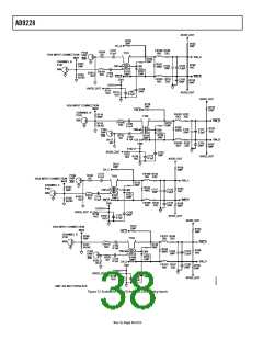
SILKSCREEN PARTITION
PIN 1 INDICATOR
Figure 69. Typical PCB Layout
Rev. 0 | Page 3ꢁ of 52

 ADI [ ADI ]