AD9228
50 Ω terminated and ac-coupled to handle single-ended
sine wave types of inputs. The transformer converts the
single-ended input to a differential signal that is clipped
before entering the ADC clock inputs.
DEFAULT OPERATION AND JUMPER SELECTION
SETTINGS
The following is a list of the default and optional settings or
modes allowed on the AD9228 Rev. A evaluation board.
A differential LVPECL clock can also be used to clock the
ADC input using the AD9515 (U202). Simply populate
R225 and R227 with 0 Ω resistors and remove R217 and
R218 to disconnect the default clock path inputs. In addition,
populate C207 and C208 with a 0.1 μF capacitor and remove
C210 and C211 to disconnect the default cloth path outputs.
The AD9515 has many pin-strappable options that are set
to a default working condition. Consult the AD9515 data
sheet for more information about these and other options.
•
•
POWER: Connect the switching power supply that is
supplied in the evaluation kit between a rated 100 V ac
to 240 V ac wall outlet at 47 Hz to 63 Hz and P503.
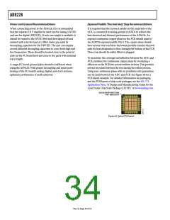
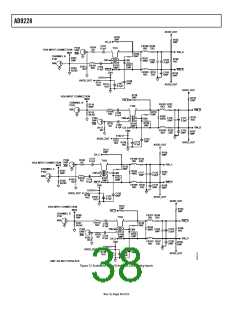
AIN: The evaluation board is set up for a transformer-
coupled analog input with optimum 50 Ω impedance
matching out to 200 MHz (see Figure 71). For more
bandwidth response, the differential capacitor across the
analog inputs can be changed or removed. The common
mode of the analog inputs is developed from the center
tap of the transformer or AVDD_DUT/2.
If using an oscillator, two oscillator footprint options are
also available (OSC201) to check the ADC performance.
J205 gives the user flexibility in using the enable pin, which
is common on most oscillators.
0
–2
–3dB CUTOFF = 200MHz
–4
–6
•
•
PDWN: To enable the power-down feature, simply short
J201 to the on position (AVDD) on the PDWN pin.
SCLK/DTP: To enable one of the two digital test patterns
on the digital outputs of the ADC, use J204. If J204 is tied to
AVDD during device power-up, Test Pattern 1000 0000 0000
will be enabled. See the SCLK/DTP Pin section for details.
–8
–10
–12
–14
–16
•
SDIO/ODM: To enable the low power, reduced signal option
similar to the IEEE 1595.3 reduced range link LVDS output
standard, use J203. If J203 is tied to AVDD during device
power-up, it enables the LVDS outputs in a low power,
reduced signal option from the default ANSI standard.
This option changes the signal swing from 350 mV p-p to
200 mV p-p, which reduces the power of the DRVDD supply.
See the SDIO/ODM Pin section for more details.
0
50
100 150 200 250 300 350 400 450 500
FREQUENCY (MHz)
Figure 71. Evaluation Board Full Power Bandwidth
•
VREF: VREF is set to 1.0 V by tying the SENSE pin to
ground, R237. This causes the ADC to operate in 2.0 V p-p
full-scale range. A separate external reference option using
the ADR510 or ADR520 is also included on the evaluation
board. Simply populate R231 and R235 and remove C214.
Proper use of the VREF options is noted in the Voltage
Reference section.
•
•
CSB: To enable the SPI information on the SDIO and
SCLK pins that is to be processed, simply tie J202 low in
the always enable mode. To ignore the SDIO and SCLK
information, tie J202 to AVDD.
•
•
RBIAS: RBIAS has a default setting of 10 kΩ (R201) to
ground and is used to set the ADC core bias current. To
further lower the core power (excluding the LVDS driver
supply), simply change the resistor setting. However,
performance of the ADC will degrade depending on the
resistor chosen. See RBIAS section for more information.
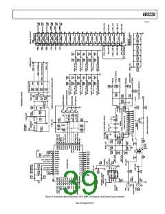
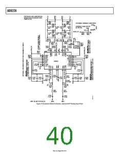
D+, D−: If an alternative data capture method to the setup
described in Figure 72 is used, optional receiver terminations,
R206 to R211, can be installed next to the high speed back-
plane connector.
CLOCK: The default clock input circuitry is derived from a
simple transformer-coupled circuit using a high bandwidth
1:1 impedance ratio transformer (T201) that adds a very
low amount of jitter to the clock path. The clock input is
Rev. 0 | Page 3ꢃ of 52

 ADI [ ADI ]