AD9228
By asserting the PDWN pin high, the AD9228 is placed in
power-down mode. In this state, the ADC typically dissipates
3 mW. During power-down, the LVDS output drivers are placed in
a high impedance state. The AD9228 returns to normal operating
mode when the PDWN pin is pulled low. This pin is both 1.8 V
and 3.3 V tolerant.
100 Ω termination resistor placed as close to the receiver as
possible. No far-end receiver termination and poor differential
trace routing may result in timing errors. It is recommended
that the trace length is no longer than 24 inches and that the
differential output traces are kept close together and at equal
lengths. An example of the FCO and data stream with proper
trace length and position can be found in Figure 58.
In power-down mode, low power dissipation is achieved by
shutting down the reference, reference buffer, PLL, and biasing
networks. The decoupling capacitors on REFT and REFB are
discharged when entering power-down mode and must be
recharged when returning to normal operation. As a result, the
wake-up time is related to the time spent in the power-down
mode; shorter cycles result in proportionally shorter wake-up
times. With the recommended 0.1 ꢀF and 2.2 ꢀF decoupling
capacitors on REFT and REFB, it takes approximately 1 sec to
fully discharge the reference buffer decoupling capacitors and
375 ꢀs to restore full operation.
There are a number of other power-down options available
when using the SPI port interface. The user can individually
power down each channel or put the entire device into standby
mode. This allows the user to keep the internal PLL powered
when fast wake-up times (~600 ns) are required. See the
Memory Map section for more details on using these features.
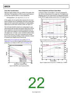
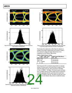
2.5ns/DIV
CH1 200mV/DIV = DCO
CH2 200mV/DIV = DATA
CH3 500mV/DIV = FCO
Figure 58. LVDS Output Timing Example in ANSI Mode (Default)
An example of the LVDS output using the ANSI standard (default)
data eye and a time interval error (TIE) jitter histogram with
trace lengths less than 24 inches on regular FR-4 material is
shown in Figure 59. Figure 60 shows an example of when the
trace lengths exceed 24 inches on regular FR-4 material. Notice
that the TIE jitter histogram reflects the decrease of the data eye
opening as the edge deviates from the ideal position. It is up to
the user to determine if the waveforms meet the timing budget
of the design when the trace lengths exceed 24 inches. Additional
SPI options allow the user to further increase the internal ter-
mination (increasing the current) of all four outputs in order to
drive longer trace lengths (see Figure 61). Even though this
produces sharper rise and fall times on the data edges and is less
prone to bit errors, the power dissipation of the DRVDD supply
increases when this option is used. Also notice in Figure 61 that
the histogram has improved. See the Memory Map section for
more details.
Digital Outputs and Timing
The AD9228 differential outputs conform to the ANSI-644
LVDS standard on default power-up. This can be changed to a
low power, reduced signal option similar to the IEEE 1596.3
standard using the SDIO/ODM pin or via the SPI. This LVDS
standard can further reduce the overall power dissipation of the
device by roughly 15 mW. See the SDIO/ODM Pin section or
Table 15 in the Memory Map section for more information. The
LVDS driver current is derived on-chip and sets the output
current at each output equal to a nominal 3.5 mA. A 100 Ω
differential termination resistor placed at the LVDS receiver
inputs results in a nominal 350 mV swing at the receiver.
The AD9228 LVDS outputs facilitate interfacing with LVDS
receivers in custom ASICs and FPGAs that have LVDS capability
for superior switching performance in noisy environments.
Single point-to-point net topologies are recommended with a
Rev. 0 | Page 23 of 52

 ADI [ ADI ]