AD9228
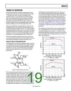
ADT1–1WT
1:1 Z RATIO
For best dynamic performance, the source impedances driving
VIN+ and VIN− should be matched such that common-mode
settling errors are symmetrical. These errors are reduced by the
common-mode rejection of the ADC. An internal reference
buffer creates the positive and negative reference voltages, REFT
and REFB, respectively, that define the span of the ADC core.
The output common-mode of the reference buffer is set to
midsupply, and the REFT and REFB voltages and span are
defined as
C
R
VIN+
VIN–
ADC
2Vp-p
49.9ꢀ
*C
R
DIFF
AD9228
AVDD
1kꢀ
AGND
C
*C
DIFF IS OPTIONAL
1kꢀ
0.1μF
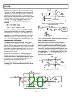
Figure 46. Differential Transformer Coupled Configuration
for Baseband Applications
REFT = 1/2 (AVDD + VREF)
REFB = 1/2 (AVDD − VREF)
Span = 2 × (REFT − REFB) = 2 × VREF
ADT1–1WT
1:1 Z RATIO
2Vp-p
16nH
16nH 0.1μF
33ꢀ
VIN+
65ꢀ
ADC
AD9228
499ꢀ
16nH
2.2pF
1kꢀ
It can be seen from these equations that the REFT and REFB
voltages are symmetrical about the midsupply voltage and, by
definition, the input span is twice the value of the VREF voltage.
33ꢀ
VIN–
AVDD
1kꢀ
Maximum SNR performance is always achieved by setting the
ADC to the largest span in a differential configuration. In the
case of the AD9228, the largest input span available is 2 V p-p.
0.1μF
1kꢀ
Figure 47. Differential Transformer Coupled Configuration for IF Applications
Differential Input Configurations
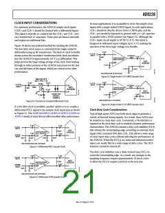
Single-Ended Input Configuration
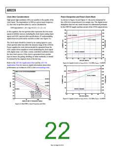
There are several ways in which to drive the AD9228 either
actively or passively. In either case, the optimum performance is
achieved by driving the analog input differentially. One example
is by using the AD8332 differential driver. It provides excellent
performance and a flexible interface to the ADC (see Figure 49)
for baseband applications. This configuration is common for
medical ultrasound systems.
A single-ended input may provide adequate performance in
cost-sensitive applications. In this configuration, SFDR and
distortion performance degrade due to the large input common-
mode swing. If the application requires a single-ended input
configuration, ensure that the source impedances on each input
are well matched in order to achieve the best possible performance.
A full-scale input of 2 V p-p can still be applied to the ADC’s VIN+
pin while the VIN− pin is terminated. Figure 48 details a typical
single-ended input configuration.
However, the noise performance of most amplifiers is not
adequate to achieve the true performance of the AD9228. For
applications where SNR is a key parameter, differential transfor-
mer coupling is the recommended input configuration. Two
examples are shown in Figure 46 and Figure 47.
AVDD
C
R
VIN+
0.1µF
AVDD
1kꢀ
25ꢀ
2V p-p
49.9ꢀ
ADC
AD9228
*C
In any configuration, the value of the shunt capacitor, C, is
dependent on the input frequency and may need to be reduced
or removed.
DIFF
1kꢀ
R
C
VIN–
0.1µF
1kꢀ
*C
DIFF IS OPTIONAL
Figure 48. Single-Ended Input Configuration
0.1μF
LOP
VIP
0.1μF
187ꢀ
374ꢀ
R
VOH
VOL
0.1μF 120nH
INH
VIN+
1V p-p
AD8332
1.0kꢀ
22pF
LNA
ADC
AD9228
VGA
C
1.0kꢀ
R
LMD
VIN–
VREF
0.1μF
187ꢀ
0.1μF
0.1μF
10μF
LON
VIN
274ꢀ
18nF
0.1μF
Figure 49. Differential Input Configuration Using the AD8332
Rev. 0 | Page 20 of 52

 ADI [ ADI ]