AD9228
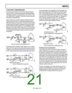
Two output clocks are provided to assist in capturing data from
the AD9228. The DCO is used to clock the output data and is
equal to six times the sampling clock (CLK) rate. Data is
clocked out of the AD9228 and must be captured on the rising
and falling edges of the DCO that supports double data rate
(DDR) capturing. The frame clock out (FCO) is used to signal
the start of a new output byte and is equal to the sampling clock
rate. See the timing diagram shown in Figure 2 for more
information.
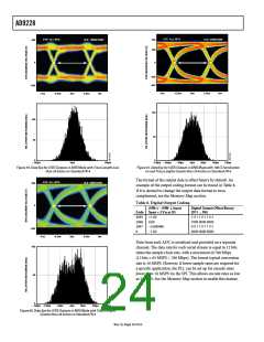
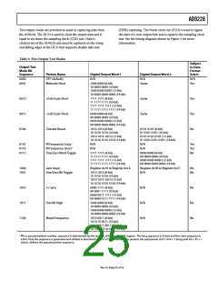
Table 9. Flex Output Test Modes
Subject
to Data
Format
Output Test
Mode Bit
Sequence
Pattern Name
OFF (default)
Midscale Short
Digital Output Word 1
Digital Output Word 2
Select
0000
0001
N/A
N/A
Same
N/A
Yes
1000 0000 (ꢀ-bit)
10 0000 0000 (10-bit)
1000 0000 0000 (12-bit)
10 0000 0000 0000 (1ꢁ-bit)
0010
0011
0100
+Full-Scale Short
−Full-Scale Short
Checker Board
1111 1111 (ꢀ-bit)
Same
Same
Yes
Yes
No
11 1111 1111 (10-bit)
1111 1111 1111 (12-bit)
11 1111 1111 1111 (1ꢁ-bit)
0000 0000 (ꢀ-bit)
00 0000 0000 (10-bit)
0000 0000 0000 (12-bit)
00 0000 0000 0000 (1ꢁ-bit)
1010 1010 (ꢀ-bit)
0101 0101 (ꢀ-bit)
10 1010 1010 (10-bit)
1010 1010 1010 (12-bit)
10 1010 1010 1010 (1ꢁ-bit)
N/A
N/A
01 0101 0101 (10-bit)
0101 0101 0101 (12-bit)
01 0101 0101 0101 (1ꢁ-bit)
N/A
N/A
0101
0110
0111
PN Sequence Long1
PN Sequence Short1
One/Zero Word Toggle
Yes
Yes
No
1111 1111 (ꢀ-bit)
0000 0000 (ꢀ-bit)
11 1111 1111 (10-bit)
1111 1111 1111 (12-bit)
11 1111 1111 1111 (1ꢁ-bit)
00 0000 0000 (10-bit)
0000 0000 0000 (12-bit)
00 0000 0000 0000 (1ꢁ-bit)
1000
1001
User Input
One/Zero Bit Toggle
Register 0x19 to Register 0x1A
1010 1010 (ꢀ-bit)
Register 0x1B to Register 0x1C
N/A
No
No
10 1010 1010 (10-bit)
1010 1010 1010 (12-bit)
10 1010 1010 1010 (1ꢁ-bit)
1010
1011
1100
1× Sync
0000 1111 (ꢀ-bit)
N/A
N/A
N/A
No
No
No
00 0001 1111 (10-bit)
0000 0011 1111 (12-bit)
00 0000 0111 1111 (1ꢁ-bit)
One Bit High
Mixed Frequency
1000 0000 (ꢀ-bit)
10 0000 0000 (10-bit)
1000 0000 0000 (12-bit)
10 0000 0000 0000 (1ꢁ-bit)
1010 0011 (ꢀ-bit)
10 0110 0011 (10-bit)
1010 0011 0011 (12-bit)
10 1000 0110 0111 (1ꢁ-bit)
1 PN, or pseudorandom number, sequence is determined by the number of bits in the shift register. The long sequence is 23 bits and the short sequence is
9 bits. How the sequence is generated and utilized is described in the ITU O.150 standard. In general, the polynomial, X23 + X1ꢀ + 1 (long) and X9 + X5 + 1
(short), defines the pseudorandom sequence.
Rev. 0 | Page 25 of 52

 ADI [ ADI ]