AD9228
Clock Jitter Considerations
Power Dissipation and Power-Down Mode
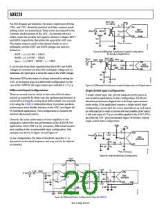
High speed, high resolution ADCs are sensitive to the quality of the
clock input. The degradation in SNR at a given input frequency
(fA) due only to aperture jitter (tJ) can be calculated by
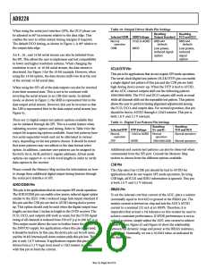
As shown in Figure 56 and Figure 57, the power dissipated by
the AD9228 is proportional to its sample rate. The digital power
dissipation does not vary much because it is determined primarily
by the DRVDD supply and bias current of the LVDS output drivers.
SNR degradation = 20 × log 10 [1/2 × π × fA × tJ]
180
160
140
120
100
80
360
340
320
300
280
260
240
220
200
180
In this equation, the rms aperture jitter represents the root mean
square of all jitter sources, including the clock input, analog input
signal, and ADC aperture jitter specifications. IF undersampling
applications are particularly sensitive to jitter (see Figure 55).
AVDD CURRENT
TOTAL POWER
The clock input should be treated as an analog signal in cases
where aperture jitter may affect the dynamic range of the AD9228.
Power supplies for clock drivers should be separated from the
ADC output driver supplies to avoid modulating the clock signal
with digital noise. Low jitter, crystal-controlled oscillators make
the best clock sources. If the clock is generated from another
type of source (by gating, dividing, or other methods), it should
be retimed by the original clock at the last step.
60
40
DRVDD CURRENT
20
0
10
15
20
25
30
35
40
ENCODE (MSPS)
Refer to the AN-501 Application Note and the AN-756
Application Note for more in-depth information about jitter
performance as it relates to ADCs (visit www.analog.com).
Figure 56. Supply Current vs. fSAMPLE for fIN = 10.3 MHz, fSAMPLE = 40 MSPS
250
480
460
440
420
400
380
360
340
320
300
130
AVDD CURRENT
200
RMS CLOCK JITTER REQUIREMENT
120
110
TOTAL POWER
150
100
16 BITS
100
90
80
70
60
50
40
14 BITS
12 BITS
50
0
10 BITS
DRVDD CURRENT
0.125 ps
0.25 ps
0.5 ps
10
20
30
40
50
60
1.0 ps
ENCODE (MSPS)
2.0 ps
30
1
Figure 57. Supply Current vs. fSAMPLE for fIN = 10.3 MHz, fSAMPLE = 65 MSPS
10
100
1000
ANALOG INPUT FREQUENCY (MHz)
Figure 55. Ideal SNR vs. Input Frequency and Jitter
Rev. 0 | Page 22 of 52

 ADI [ ADI ]