AD9228
90
85
80
75
70
65
75
70
65
60
55
50
Internal Reference Operation
A comparator within the AD9228 detects the potential at the
SENSE pin and configures the reference. If SENSE is grounded,
the reference amplifier switch is connected to the internal
resistor divider (see Figure 64), setting VREF to 1 V.
SNR
SFDR
The REFT and REFB pins establish their input span of the ADC
core from the reference configuration. The analog input full-
scale range of the ADC equals twice the voltage at the reference
pin for either an internal or an external reference configuration.
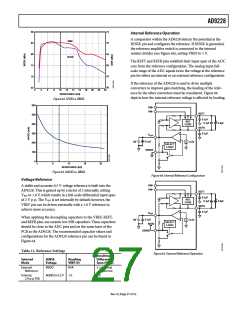
If the reference of the AD9228 is used to drive multiple
converters to improve gain matching, the loading of the refer-
ence by the other converters must be considered. Figure 66
depicts how the internal reference voltage is affected by loading.
2
4
6
8
10
12
14
16
18
20
22
24
RESISTANCE (kꢀ)
Figure 62. SFDR vs. RBIAS
600
500
400
300
200
100
0
VIN+
VIN–
REFT
0.1µF
+
ADC
CORE
0.1µF
2.2µF
REFB
0.1µF
V
REF
1µF
0.1µF
0.5V
SELECT
LOGIC
SENSE
3
8
13
18
23
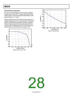
RESISTANCE (kꢀ)
Figure 63. IAVDD vs. RBIAS
Figure 64. Internal Reference Configuration
Voltage Reference
VIN+
VIN–
A stable and accurate 0.5 V voltage reference is built into the
AD9228. This is gained up by a factor of 2 internally, setting
REFT
V
REF to 1.0 V, which results in a full-scale differential input span
0.1µF
0.1µF
REFB
+
ADC
CORE
of 2 V p-p. The VREF is set internally by default; however, the
VREF pin can be driven externally with a 1.0 V reference to
achieve more accuracy.
2.2µF
0.1µF
V
REF
When applying the decoupling capacitors to the VREF, REFT,
and REFB pins, use ceramic low ESR capacitors. These capacitors
should be close to the ADC pins and on the same layer of the
PCB as the AD9228. The recommended capacitor values and
configurations for the AD9228 reference pin can be found in
Figure 64.
1µF
0.1µF
AVDD
0.5V
SELECT
LOGIC
SENSE
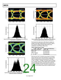
Table 12. Reference Settings
Figure 65. External Reference Operation
Resulting
Selected
Mode
SENSE
Voltage
Resulting
VREF (V)
Differential
Span (V p-p)
External
AVDD
N/A
2 × external
reference
Reference
Internal,
2 V p-p FSR
AGND to 0.2 V
1.0
2.0
Rev. 0 | Page 2ꢂ of 52

 ADI [ ADI ]