AD9228
CLOCK INPUT CONSIDERATIONS
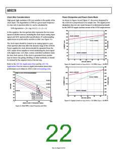
In some applications, it is acceptable to drive the sample clock
inputs with a single-ended CMOS signal. In such applications,
CLK+ should be directly driven from a CMOS gate, and the
CLK− pin should be bypassed to ground with a 0.1 μF capacitor
in parallel with a 39 kΩ resistor (see Figure 53). Although the
CLK+ input circuit supply is AVDD (1.8 V), this input is
designed to withstand input voltages up to 3.3 V, making the
selection of the drive logic voltage very flexible.
For optimum performance, the AD9228 sample clock inputs
(CLK+ and CLK−) should be clocked with a differential signal.
This signal is typically ac-coupled into the CLK+ and CLK− pins
via a transformer or capacitors. These pins are biased internally
and require no additional bias.
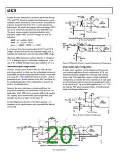
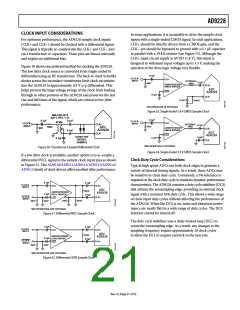
Figure 50 shows one preferred method for clocking the AD9228.
The low jitter clock source is converted from single-ended to
differential using an RF transformer. The back-to-back Schottky
diodes across the secondary transformer limit clock excursions
into the AD9228 to approximately 0.8 V p-p differential. This
helps prevent the large voltage swings of the clock from feeding
through to other portions of the AD9228 and preserves the fast
rise and fall times of the signal, which are critical to low jitter
performance.
0.1µF
CLOCK
CLK
INPUT
OPTIONAL
100ꢀ
0.1µF
50ꢀ*
AD9510/1/2/3/4/5
CMOS DRIVER
CLK+
ADC
AD9228
CLK
0.1µF
CLK–
0.1µF
39kꢀ
*50ꢀ RESISTOR IS OPTIONAL
Figure 53. Single-Ended 1.8 V CMOS Sample Clock
MIN-CIRCUITS
ADT1–1WT, 1:1Z
0.1µF
CLK
0.1µF
0.1µF
CLOCK
INPUT
XFMR
CLOCK
INPUT
CLK+
OPTIONAL
0.1µF
50ꢀ*
100ꢀ
100ꢀ
ADC
AD9228
CLK–
AD9510/1/2/3/4/5
CMOS DRIVER
50ꢀ
CLK+
0.1µF
ADC
AD9228
CLK
SCHOTTKY
DIODES:
0.1µF
0.1µF
0.1µF
CLK–
HSM2812
*50ꢀ RESISTOR IS OPTIONAL
Figure 50. Transformer Coupled Differential Clock
Figure 54. Single-Ended 3.3 V CMOS Sample Clock
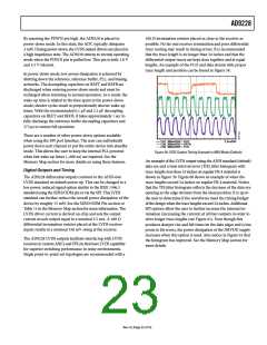
If a low jitter clock is available, another option is to ac-couple a
differential PECL signal to the sample clock input pins as shown
in Figure 51. The AD9510/AD9511/AD9512/AD9513/AD9514/
AD9515 family of clock drivers offers excellent jitter performance.
Clock Duty Cycle Considerations
Typical high speed ADCs use both clock edges to generate a
variety of internal timing signals. As a result, these ADCs may
be sensitive to clock duty cycle. Commonly, a 5% tolerance is
required on the clock duty cycle to maintain dynamic performance
characteristics. The AD9228 contains a duty cycle stabilizer (DCS)
that retimes the nonsampling edge, providing an internal clock
signal with a nominal 50% duty cycle. This allows a wide range
of clock input duty cycles without affecting the performance of
the AD9228. When the DCS is on, noise and distortion perfor-
mance are nearly flat for a wide range of duty cycles. The DCS
function cannot be turned off.
0.1µF
0.1µF
CLOCK
INPUT
CLK
CLK+
ADC
AD9228
100ꢀ
AD9510/1/2/3/4/5
PECL DRIVER
0.1µF
0.1µF
CLOCK
INPUT
CLK–
CLK
240ꢀ
240ꢀ
50ꢀ*
50ꢀ*
*50ꢀ RESISTORS ARE OPTIONAL
Figure 51. Differential PECL Sample Clock
The duty cycle stabilizer uses a delay-locked loop (DLL) to
create the nonsampling edge. As a result, any changes to the
sampling frequency require approximately 10 clock cycles
to allow the DLL to acquire and lock to the new rate.
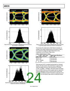
0.1µF
0.1µF
CLOCK
INPUT
CLK+
CLK
ADC
AD9228
100ꢀ
AD9510/1/2/3/4/5
LVDS DRIVER
0.1µF
0.1µF
CLOCK
INPUT
CLK–
CLK
50ꢀ*
50ꢀ*
*50ꢀ RESISTORS ARE OPTIONAL
Figure 52. Differential LVDS Sample Clock
Rev. 0 | Page 21 of 52

 ADI [ ADI ]