AD9228
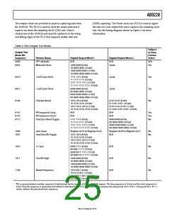
Table 10. Output Driver Mode Pin Settings
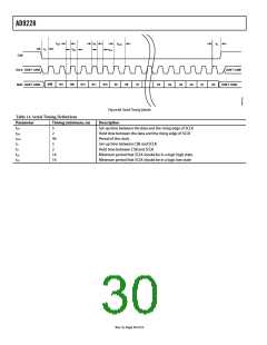
When using the serial port interface (SPI), the DCO phase can
be adjusted in 60° increments relative to the data edge. This
enables the user to refine system timing margins if required.
The default DCO timing, as shown in Figure 2, is 90° relative to
the output data edge.
Resulting
Resulting
Selected ODM ODM Voltage
Normal
operation
Output Standard FCO and DCO
10 kΩ to AGND ANSI-ꢃꢁꢁ
ANSI-ꢃꢁꢁ
(default)
(default)
ODM
AVDD
Low power,
reduced signal
option
Low power,
reduced
signal
An 8-, 10-, and 14-bit serial stream can also be initiated from
the SPI. This allows the user to implement and test compatibility
to lower and higher resolution systems. When changing the
resolution to an 8- or 10-bit serial stream, the data stream is
shortened. See Figure 3 for the 10-bit example. However, when
using the 14-bit option, the data stream stuffs two 0s at the end
of the normal 14-bit serial data.
option
SCLK/DTP Pin
This pin is for applications that do not require SPI mode operation.
The serial clock/digital test pattern (SCLK/DTP) pin can enable
a single digital test pattern if this pin and the CSB pin are held
high during device power-up. When the DTP is tied to AVDD,
all the ADC channel outputs shift out the following pattern:
1000 0000 0000. The FCO and DCO outputs still work as usual
while all channels shift out the repeatable test pattern. This pattern
allows the user to perform timing alignment adjustments among
the FCO, DCO, and output data. For normal operation, this pin
should be tied to AGND through a 10 kΩ resistor. This pin is
both 1.8 V and 3.3 V tolerant.
When using the SPI, all of the data outputs can also be inverted
from their nominal state. This is not to be confused with
inverting the serial stream to an LSB-first mode. In default
mode, as shown in Figure 2, the MSB is represented first in the
data output serial stream. However, this can be inverted so that
the LSB is represented first in the data output serial stream (see
Figure 4).
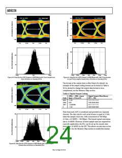
There are 12 digital output test pattern options available that
can be initiated through the SPI. This is a useful feature when
validating receiver capture and timing. Refer to Table 9 for the
output bit sequencing options available. Some test patterns have
two serial sequential words and can be alternated in various
ways, depending on the test pattern chosen. It should be noted
that some patterns may not adhere to the data format select
option. In addition, customer user patterns can be assigned in
the 0x19, 0x1A, 0x1B, and 0x1C register addresses. All test mode
options can support 8- to 14-bit word lengths in order to verify
data capture to the receiver.
Table 11. Digital Test Pattern Pin Settings
Resulting
Resulting
FCO and DCO
Selected DTP DTP Voltage
Normal
operation
DTP
D+ and D−
10 kΩ to AGND Normal
Normal operation
operation
AVDD
1000 0000 0000 Normal operation
Additional and custom test patterns can also be observed when
commanded from the SPI port. Consult the Memory Map
section to choose from the different options available.
CSB Pin
Please consult the Memory Map section for information on how
to change these additional digital output timing features through
the serial port interface or SPI.
The chip select bar (CSB) pin should be tied to AVDD for
applications that do not require SPI mode operation. By tying
CSB high, all SCLK and SDIO information is ignored. This pin
is both 1.8 V and 3.3 V tolerant.
SDIO/ODM Pin
RBIAS Pin
This pin is for applications that do not require SPI mode operation.
The SDIO/ODM pin can enable a low power, reduced signal option
similar to the IEEE 1596.3 reduced range link output standard if
this pin and the CSB pin are tied to AVDD during device power-
up. This option should only be used when the digital output trace
lengths are less than 2 inches in length to the LVDS receiver. The
FCO, DCO, and outputs still work as usual, but the LVDS signal
swing of all channels is reduced from 350 mV p-p to 200 mV p-p.
This output mode allows the user to further lower the power on
the DRVDD supply. For applications where this pin is not used,
it should be tied low. In this case, the device pin can be left open,
and the 30 kΩ internal pull-down resistor pulls this pin low. This
pin is only 1.8 V tolerant. If applications require this pin to be
driven from a 3.3 V logic level, insert a 1 kΩ resistor in series
with this pin to limit the current.
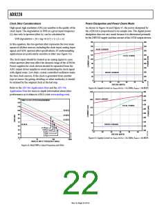
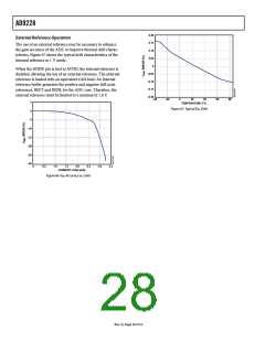
To set the internal core bias current of the ADC, place a resistor
(nominally equal to 10.0 kΩ) to ground at the RBIAS pin. The
resistor current is derived on-chip and sets the ADC’s AVDD
current to a nominal 232 mA at 65 MSPS. Therefore, it is
imperative that at least a 1% tolerance on this resistor be used to
achieve consistent performance. If SFDR performance is not as
critical as power, simply adjust the ADC core current to achieve
a lower power. Figure 62 and Figure 63 show the relationship
between the dynamic range and power as the RBIAS resistance
is changed. Nominally, we use a 10.0 kΩ value, as indicated by
the dashed line.
Rev. 0 | Page 2ꢃ of 52

 ADI [ ADI ]