AD9228
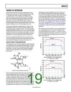
THEORY OF OPERATION
realizing the maximum bandwidth of the ADC. Such use of
The AD9228 architecture consists of a pipelined ADC that is
divided into three sections: a 4-bit first stage followed by eight
1.5-bit stages and a final 3-bit flash. Each stage provides
sufficient overlap to correct for flash errors in the preceding
stages. The quantized outputs from each stage are combined
into a final 12-bit result in the digital correction logic. The
pipelined architecture permits the first stage to operate on a
new input sample while the remaining stages operate on preceding
samples. Sampling occurs on the rising edge of the clock.
low-Q inductors or ferrite beads is required when driving the
converter front end at high IF frequencies. Either a shunt capacitor
or two single-ended capacitors can be placed on the inputs to
provide a matching passive network. This ultimately creates a
low-pass filter at the input to limit any unwanted broadband
noise. See the AN-742 Application Note, the AN-827 Application
Note, and the Analog Dialogue article “Transformer-Coupled
Front-End for Wideband A/D Converters” for more information
on this subject. In general, the precise values depend on the
application.
Each stage of the pipeline, excluding the last, consists of a low
resolution flash ADC connected to a switched-capacitor DAC
and interstage residue amplifier (MDAC). The residue amplifier
magnifies the difference between the reconstructed DAC output
and the flash input for the next stage in the pipeline. One bit of
redundancy is used in each stage to facilitate digital correction
of flash errors. The last stage simply consists of a flash ADC.
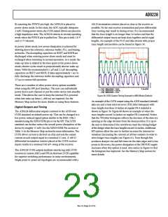
The analog inputs of the AD9228 are not internally dc-biased.
In ac-coupled applications, the user must provide this bias
externally. Setting the device so that VCM = AVDD/2 is recom-
mended for optimum performance, but the device can function
over a wider range with reasonable performance, as shown in
Figure 44 and Figure 45.
The output staging block aligns the data, carries out the error
correction, and passes the data to the output buffers. The data is
then serialized and aligned to the frame and output clock.
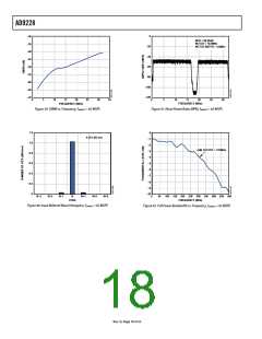
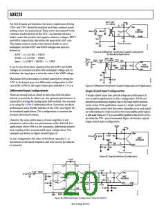
90
SFDR (dBc)
85
80
ANALOG INPUT CONSIDERATIONS
75
The analog input to the AD9228 is a differential switched-capacitor
circuit designed for processing differential input signals. The input
can support a wide common-mode range and maintain excellent
performance. An input common-mode voltage of midsupply
minimizes signal-dependent errors and provides optimum
performance.
SNR (dB)
70
65
60
55
50
0.2
0.4
0.6
0.8
1.0
1.2
1.4
1.6
H
ANALOG INPUT COMMON MODE VOLTAGE (V)
Figure 44. SNR/SFDR vs. Common-Mode Voltage,
fIN = 2.4 MHz, fSAMPLE = 65 MSPS
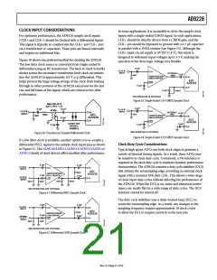
CPAR
H
VIN+
CSAMPLE
90
S
S
S
S
SFDR (dBc)
85
80
75
70
65
60
55
50
CSAMPLE
VIN–
H
CPAR
H
SNR (dB)
Figure 43. Switched-Capacitor Input Circuit
The clock signal alternately switches the input circuit between
sample mode and hold mode (see Figure 43). When the input
circuit is switched into sample mode, the signal source must be
capable of charging the sample capacitors and settling within
one-half of a clock cycle. A small resistor in series with each
input can help reduce the peak transient current injected from
the output stage of the driving source. In addition, low-Q inductors
or ferrite beads can be placed on each leg of the input to reduce
the high differential capacitance seen at the analog inputs, thus
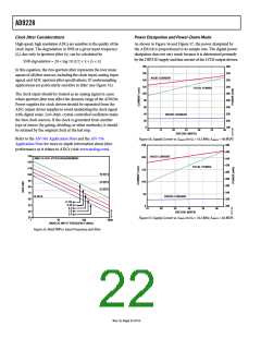
0.8
0.2
0.4
0.6
1.0
1.2
1.4
1.6
ANALOG INPUT COMMON MODE VOLTAGE (V)
Figure 45. SNR/SFDR vs. Common-Mode Voltage,
f
IN = 30 MHz, fSAMPLE = 65 MSPS
Rev. 0 | Page 19 of 52

 ADI [ ADI ]