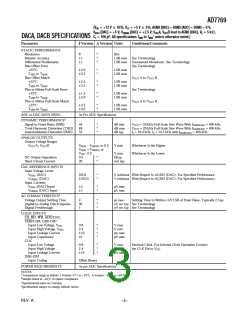
AD7769
P lus and Minus Full-Scale Er r or
Signal-to-Noise Ratio (SNR)
The ADC and DACs in the AD7769 can be considered as de-
vices with bipolar (plus and minus) input ranges, but referred to
VBIAS instead of AGND. Plus Full-Scale Error for the ADC is the
difference between the actual input voltage at the FE to FF code
transition and the ideal input voltage (VBIAS + VSWING –1.5 LSB),
expressed in LSBs. Minus Full-Scale Error is similarly specified
for the 01 to 00 code transition, relative to the ideal input voltage
for this transition (VBIAS – VSWING +0.5 LSB). Plus Full-Scale
Error for the DACs is the difference, expressed in LSBs, between
the actual output voltage for input code FF and the ideal voltage
(VBIAS + VSWING – 1 LSB). Minus Full-Scale Error is similarly
SNR is the measured Signal-to-Noise Ratio at the output of the
converter. T he signal is the rms magnitude of the fundamental.
Noise is the rms sum of all the nonfundamental signals up to
half the sampling frequency. SNR is dependent on the number
of quantization levels used in the digitization process; the more
levels, the smaller the quantization noise. T he theoretical SNR
for a sine wave is given by
SNR = (6.02N + 1.76) dB
where N is the number of bits. T hus for an ideal 8-bit converter,
SNR = 49.92 dB.
specified for code 00, relative to the ideal output voltage (VBIAS
SWING). Note that Plus and Minus Full-Scale errors for the
ADC and the DAC outputs are measured after their respective
Bias Offset errors have been adjusted out.
–
Total H ar m onic D istor tion (TH D )
T HD is the ratio of the rms sum of harmonics to the fundamen-
tal. For the AD7769, T otal Harmonic Distortion is defined as
V
1/2
(V22 + V32 + V42 + V52 + V6 )
2
D igital-to-Analog Glitch Im pulse
20 log
V1
Digital-to-Analog Glitch Impulse is the impulse injected into the
analog outputs when the digital inputs change state with either
DAC selected. It is normally specified as the area of the glitch in
nV secs and is measured when the digital input code is changed
by 1 LSB at the major carry transition.
where V1 is the rms amplitude of the fundamental and V2,
V3, V4, V5 and V6 are the rms amplitudes of the individual
harmonics.
Inter m odulation D istor tion (IMD )
D igital Feedthr ough
With inputs consisting of sine waves at two frequencies, fa and
fb, any active device with nonlinearities will create distortion
products, of order (m+n), at sum and difference frequencies of
mfa+nfb, where m, n = 0, 1, 2, 3 . . . Intermodulation terms are
those for which neither m nor n is equal to zero. For example,
the second order terms include (fa+fb) and (fa–fb) and the third
order terms include (2fa+fb), (2fa–fb), (fa+2fb) and (fa–2fb).
Digital Feedthrough is also a measure of the impulse injected
into the analog outputs from the digital inputs but is measured
when the DACs are not selected. T his is essentially feedthrough
across the die and package. It is important in the AD7769 since
it is a measure of the glitch impulse transferred to the analog
outputs when data is read from the ADC register. It is specified
in nV secs and measured with WR high and a digital code
change from all 0s to all 1s.
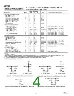
LO GIC TRUTH TABLE
AD C CH ANNEL SELECT AND START CO NVERSIO N
CS
ADC/D AC
CHA/CH B
WR
RD
D B0–D B7 INT
Com m ents
0
0
0
0
0
0
X
0
1
Note 1
Note 1
Note 1
Note 1
Note 1
Note 1
1
1
1
0
INT Is Set on Falling Edge of WR.
Select ADC Channel A and Start Conversion.
Select ADC Channel B and Start Conversion.
INT Goes Low at End of Conversion.
READ AD C D ATA
CS
ADC/D AC
CHA/CH B
WR
RD
D B0–D B7 INT
Com m ents
0
0
0
X
X
X
X
X
X
X
X
X
ADC Data
ADC Data
High-Z
1
1
1
INT Is Set High on Falling Edge of RD.
ADC Data on Data Bus.
Data Outputs Impedance.
0
WRITE TO D ACA O R D ACB
CS
ADC/D AC
CHA/CH B
WR
RD
D B0–D B7 INT
Com m ents
0
0
0
0
1
1
1
1
1
X
0
1
0
1
X
1
1
0
0
X
µP Data
µP Data
ADC Data
ADC Data
High-Z
N/C
N/C
N/C
N/C
N/C
µP Writing Data to DACA.
µP Writing Data to DACB.
Data from Last ADC Conversion Will Be Written to DACA.
Data from Last ADC Conversion Will Be Written to DACB.
No Operation.
X
NOT ES
1If RD = 1, DB0–DB7 will remain high impedance. If RD = 0, DB0–DB7 will output previous ADC data. T he RD input should not change during a conversion.
2X = Don’t Care.
3N/C = No Change.
REV. A
–7–

 ADI [ ADI ]