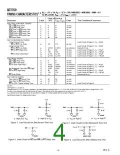
AD7769
CIRCUIT D ESCRIP TIO N
Analog Inputs and O utputs
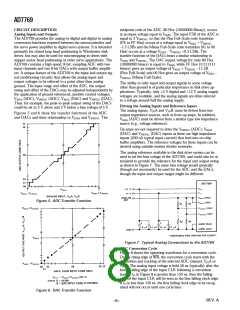
midpoint code of the ADC, 80 Hex (10000000 Binary), occurs
at an input voltage equal to VBIAS. T he input FSR of the ADC is
equal to 2 VSWING, so that the Plus Full-Scale code transition
(FE to FF Hex) occurs at a voltage equal to VBIAS + VSWING
–1.5 LSBs and the Minus Full-Scale code transition (01 to 00
Hex) occurs at a voltage VBIAS – VSWING +0.5 LSBs. T he
transfer function of the DACs bears a similar relationship to
VBIAS and VSWING. T he DAC output voltage for code 80 Hex
(10000000 binary) is equal to VBIAS, while FF Hex (11111111
binary) gives an output voltage of VBIAS + VSWING –1 LSB
The AD7769 provides the analog-to-digital and digital-to-analog
conversion functions required between the microcontroller and
the servo power amplifier in digital servo systems. It is intended
primarily for closed loop head positioning in Winchester disk
drives, but may also be used for microstepping in drives with
stepper motor head positioning or other servo applications. T he
AD7769 contains a high speed, 8-bit, sampling ADC with two
input channels and two 8-bit DACs with output buffer amplifi-
ers. A unique feature of the AD7769 is the input and output sig-
nal conditioning circuitry that allows the analog input and
output voltages to be referred to a point other than analog
ground. T he input range and offset of the ADC, the output
swing and offset of the DACs may be adjusted independently by
the application of ground-referenced, positive control voltages,
VBIAS (ADC), VSWING (ADC), VBIAS (DAC) and VSWING (DAC).
T hus, for example, the peak-to-peak output swing of the DACs
could be set to 3 V above and 3 V below a bias voltage of 5 V.
(Plus Full-Scale) and 00 Hex gives an output voltage of VBIAS
VSWING (Minus Full-Scale).
–
T he ability to refer input and output signals to some voltage
other than ground is of particular importance in disk drive ap-
plications. T ypically, only +5 V digital and +12 V analog supply
voltages are available, and the analog signals are often referred
to a voltage around half the analog supply.
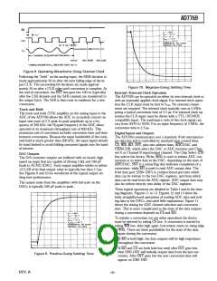
D r iving the Analog Inputs and Refer ence Inputs
T he analog inputs, VINA and VINB, must be driven from low
output impedance sources, such as from op amps. In addition,
VBIAS (ADC) must be driven from a similar type low impedance
source (e.g., voltage reference).
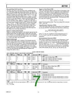
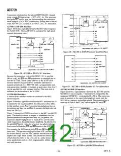
Figures 5 and 6 show the transfer functions of the ADC
and DACs and their relationship to VBIAS and VSWING. T he
Op amps are not required to drive the VSWING (ADC), VBIAS
(DAC) and VSWING (DAC) inputs as these are high impedance
inputs (200 nA typical input current) that feed into on-chip
buffer amplifiers. T he reference voltages for these inputs can be
derived using suitable resistor divider networks.
T he analog reference available in the disk drive system can be
used to set the bias voltage of the AD7769, and could also be at-
tenuated to provide the reference for the input and output swing
as shown in Figure 7. T he same bias voltage would generally
(though not necessarily) be used for the ADC and the DACs,
though the input and output ranges might be different.
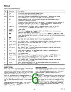
Figure 5. ADC Transfer Function
Figure 7. Typical Analog Connections to the AD7769
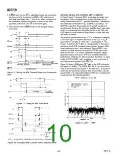
AD C Conver sion Cycle
Figure 8 shows the operating waveforms for a conversion cycle.
On the rising edge of WR, the conversion cycle starts with the
acquisition and tracking of the selected ADC channel, VINA or
VINB. T he analog input voltage is held 50 ns (typically) after the
fourth falling edge of the input CLK following a conversion
start. If tD in Figure 8 is greater than 150 ns, then the falling
edge of the input CLK will be seen as the first falling clock edge.
If tD is less than 150 ns, the first falling clock edge to be recog-
nized will not occur until one cycle later.
Figure 6. DAC Transfer Function
REV. A
–8–

 ADI [ ADI ]