AD7769
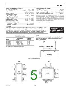
P IN FUNCTIO N D ESCRIP TIO N
P in
Mnem onic
D escription
1
VDD
+12 V Power Supply. T his powers the analog circuitry.
+5 V Power Supply. T his powers the logic circuitry.
2
VCC
3–10
DB7–DB0
Input/Output Data Bus. A bidirectional data port from which ADC output data may be read
and to which DAC input data may be written. DB7 is the Most Significant Bit.
11
12
INT
Interrupt Output (active low). INT is set high on the falling edge of RD or WR to the ADC
and goes low at the end of a conversion.
CLK
Clock input. A clock is required for the ADC. An external T T L-compatible clock may be applied to
this input pin. Alternatively, tying this pin to VDD enables the internal clock oscillator. With an
external clock, the mark-space ratio can vary from 30/70 to 70/30.
13
CHA/CHB
Channel A/Channel B Select Input. Selects Channel A or Channel B of the DAC or ADC.
Used in conjunction with WR, RD, CS and ADC/DAC for read or write operations.
14
15
DGND
Digital Ground.
ADC/DAC
ADC or DAC Select Input. Selects either the ADC or the DAC for read or write operations in
conjunction with WR, RD, CS and CHA/CHB.
16
WR
Write Input (edge triggered). T his is used in conjunction with the ADC/DAC, CHA/CHB and CS
control inputs to start an ADC conversion or write data to the DAC. An ADC conversion starts on the
rising edge of WR.
17
18
19
RD
Read Input (active low). T his input must be low to access data from the ADC.
Chip Select Input (active low). T he device is selected when this input is low.
CS
VSWING (ADC)
ADC Reference Input. T he voltage applied to this pin with respect to AGND (ADC) sets the
in put voltage Full-Scale Range (FSR) of the ADC. VIN (FSR) = 2 VSWING (ADC).
20
21
22
AGND (ADC)
ADC Analog Ground.
VINB
Analog Input for Channel B. See VINA description.
VBIAS (ADC)
ADC Reference Input. T he voltage applied to this pin with respect to AGND (ADC) sets the
midpoint of the ADC transfer function.
23
VINA
Analog Input for Channel A. T he input voltage range of both ADC channels is given by:
VIN A/B = VBIAS (ADC) ±VSWING (ADC).
24
25
AGND (DAC)
VSWING (DAC)
DAC Analog Ground.
DAC Reference Input. T he voltage applied to this pin with respect to AGND (DAC) sets the
output voltage Full-Scale Range (FSR) of the DACs. VOUT (FSR) = 2 VSWING (DAC).
26
27
VOUT
B
Analog Output Voltage from DAC B. See VOUT A description.
VBIAS (DAC)
DAC Reference Input. T he voltage applied to this pin with respect to AGND (DAC) sets the
midpoint output voltage of the DACs.
28
VOUT
A
Analog Output Voltage from DAC A. T he output voltage range of both DACs is given by:
VOUT A/B = VBIAS (DAC) ± VSWING (DAC).
TERMINO LO GY
Relative Accur acy
D iffer ential Nonlinear ity
For an ADC, Relative Accuracy or endpoint nonlinearity is the
maximum deviation, in LSBs, of the ADC’s actual code transi-
tion points from a straight line drawn between the endpoints of
the ADC transfer function, i.e., the 00 to 01 and FE to FF Hex
(01111111 to 11111111 Binary) code transitions.
Differential Nonlinearity is the difference between the measured
change and the ideal 1 LSB change between any two adjacent
codes. A specified differential nonlinearity of ±1 LSB max en-
sures monotonicity (DAC) or no missed codes (ADC).
Bias O ffset Er r or
For a DAC, Relative Accuracy or endpoint nonlinearity is a
measure of the maximum deviation, in LSBs, from a straight
line passing through the endpoints of the DAC transfer func-
tion, i.e., those voltages which correspond to codes 00 and FF
Hex.
For an ideal ADC, the output code for an input voltage equal to
VBIAS (ADC), should be 80 Hex (10000000 binary). T he ADC
Bias Offset Error is the difference between the actual midpoint
voltage for code 80 Hex and VBIAS (ADC), expressed in LSBs.
For an ideal DAC, the output voltage for code 80 Hex should
be equal to VBIAS (DAC). T he DAC Bias Offset Error is the
difference between the actual output voltage and VBIAS (DAC),
expressed in LSBs.
For the specified input and output ranges, 1 LSB = 19.5 mV,
but will vary with VSWING. For both DACs and ADC,
1 LSB = 2 VSWING /256 = FSR/256.
REV. A
–6–

 ADI [ ADI ]