AD7769
(V = +12 V ؎ 10%; V = +5 V ؎ 5%; AGND [DAC] = AGND [ADC] = DGND = 0 V;
DD
CC
BIAS [DAC] = +5 V; VSWING [DAC] = +2.5 V; V A, V B load to AGND [DAC], R = 5 k⍀,
DACA, DACB SPECIFICATIONS VC = 100 pF. All specifications TMIN to T 1 unless otherwise noted.)
OUT
OUT
L
L
MAX
P aram eter
J Version A Version Units
Conditions/Com m ents
ST AT IC PERFORMANCE
Resolution
Relative Accuracy
Differential Nonlinearity
Bias Offset Error
+25°C
8
±1
±1
*
*
*
Bits
LSB max
LSB max
See T erminology
Guaranteed Monotonic. See T erminology.
See T erminology
±2.0
±2.5
*
*
LSB max
LSB max
T MIN to T MAX
Bias Offset Match
+25°C
T MIN to T MAX
VOUT A to VOUT B
±2.5
±3.5
*
*
LSB max
LSB max
Plus or Minus Full-Scale Error
+25°C
T MIN to T MAX
See T erminology
±1.5
±2.0
*
*
LSB max
LSB max
Plus or Minus Full-Scale Match
+25°C
T MIN to T MAX
VOUT A to VOUT B
±3.5
±4.0
*
*
LSB max
LSB max
ADC to DAC MAT CHING
As Per ADC Specifications
DYNAMIC PERFORMANCE2
Signal-to-Noise Ratio (SNR)
T otal Harmonic Distortion (T HD)
Intermodulation Distortion (IMD)
44
48
55
*
*
*
dB min
dB max
dB typ
VOUT = 20 kHz Full-Scale Sine Wave With fSAMPLING = 400 kHz
VOUT = 20 kHz Full-Scale Sine Wave With fSAMPLING = 400 kHz
fa = 18.4 kHz, fb = 14.5 kHz with fSAMPLING = 400 kHz
ANALOG OUT PUT S
Output Voltage Ranges
VOUT A, VOUT
B
VBIAS – VSWING or 0.5
VBIAS + VSWING or
VDD –2.0
V min
V max
Whichever Is the Higher
Whichever Is the Lower
DC Output Impedance
Short-Circuit Current
0.5
20
*
*
Ω
mA typ
typ
DAC REFERENCE INPUT S
Input Voltage Levels
VBIAS (DAC)
3/6.8
2.0/3.0
*
*
V min/max With Respect to AGND (DAC). For Specified Performance.
V min/max With Respect to AGND (DAC). For Specified Performance.
VSWING (DAC)
Input Currents
VBIAS (DAC) Input
VSWING (DAC) Input
±2
±1
*
*
µA max
µA max
AC CHARACT ERIST ICS2
Voltage Output Settling T ime
Digital-to-Analog Glitch Impulse
Digital Feedthrough
4
30
1
*
*
*
µs max
Settling T ime to Within ±1/2 LSB of Final Value. T ypically 2.5 µs.
nV sec typ See T erminology
nV sec typ See T erminology
LOGIC INPUT S
CS, RD, WR, ADC/DAC,
CHA/CHB, DB0–DB7
Input Low Voltage, VINL
Input High Voltage, VINH
Input Leakage Current
Input Capacitance
CLK
0.8
2.4
±10
10
*
*
*
*
V max
V min
µA max
pF max
Input Low Voltage
Input High Voltage
Input Leakage Current
DB0–DB7
0.8
2.4
±10
*
*
*
V max
V min
µA max
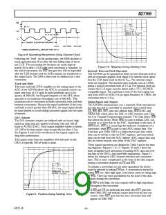
External Clock. For Internal Clock Operation Connect
the CLK Pin to VDD
.
Input Coding
Offset Binary
As per ADC Specifications
POWER REQUIREMENT S
NOT ES
1T emperature range as follows: J Version: 0°C to +70°C; A Version: –40°C to +85°C.
2Sample tested at +25°C to ensure compliance.
*Specifications same as J Version.
Specifications subject to change without notice.
REV. A
–3–

 ADI [ ADI ]