AD7769
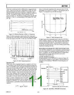
T his is for an ideal part with no differential or integral linearity
errors. T hese errors will cause a degradation in SNR. By work-
ing backwards from the above equation, it is possible to get a
measure of ADC performance expressed in effective number of
bits (N). T he effective number of bits is plotted versus fre-
quency in Figure 15. T he effective number of bits typically falls
between 7.7 and 7.9, corresponding to SNR Figures 48.1 and
49.7 dB.
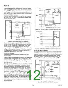
where A is the peak amplitude of the sine wave and p (V) the
probability of occurrence at a voltage V. T he histogram plot of
Figure 17 corresponds very well with this shape.
Figure 15. Effective Num ber of Bits vs. Frequency
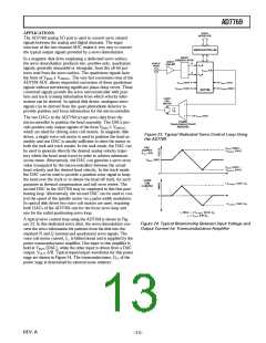
Figure 16 shows a spectrum analyzer plot of the output spec-
trum from one of the DACs with an ideal sine wave table loaded
to the data inputs of the DAC. In this case, the SNR is 47 dB.
Figure 17. ADC Histogram Plot
In digital signal processing applications, where the AD7769 is
used to sample ac signals, it is essential that the signal sampling
occurs at exactly equal intervals. T his minimizes errors due to
sampling uncertainty or jitter. A precise timer or clock source,
to start the conversion process, is the best method of generating
equidistant sampling intervals.
MICRO P RO CESSO R/MICRO CO MP UTER INTERFACING
T he AD7769 is designed for easy interfacing to microprocessors
and microcomputers as a memory mapped peripheral or an I/O
device. In addition, the AD7769 high speed bus timing allows
direct interfacing to many DSP processors such as the
T MS320C10 and ADSP-2101.
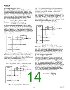
AD 7769–TMS320C10 Inter face
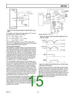
A typical interface to the T MS320C10 is shown in Figure 18.
T he AD7769 is mapped at a port address, and the interface is
designed for the maximum T MS320C10 clock frequency of
20 MHz.
Figure 16. DAC Output Spectrum
H istogr am P lot
When a sine wave of specified frequency is applied to the VIN
A
or VINB input of the AD7769 and several thousand samples are
taken, it is possible to plot a histogram showing the frequency of
occurrence of each of the 256 ADC codes. If a particular step is
wider than the ideal 1 LSB width, then the code associated with
that step will accumulate more counts than for the code for an
ideal step. Likewise, a step narrower than ideal width will have
fewer counts. Missing codes are easily seen because a missing
code means zero counts for a particular code. T he absence of
large spikes in the plot indicates small differential nonlinearity.
Figure 17 shows a histogram plot for the ADC indicating very
small differential nonlinearity and no missing codes for an input
frequency of 204 kHz. For a sine wave input, a perfect ADC
would produce a probability density function described by the
equation:
1
p (V) =
π( A2 –V 2)1/2
Figure 18. AD7769 to TMS320C10 Interface
REV. A
–11–

 ADI [ ADI ]