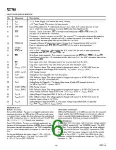
AD7769
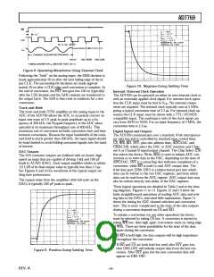
Figure 8. Operating Waveform s Using External Clock
Following the “hold” on the analog input, the MSB decision is
made approximately 50 ns after the next falling edge of the in-
put CLK. T he succeeding bit decisions are made approxi-
mately 50 ns after a CLK edge until conversion is complete. At
the end of conversion, the INT line goes low 100 ns (typically)
after the LSB decision and the SAR contents are transferred to
the output latch. T he SAR is then reset in readiness for a new
conversion.
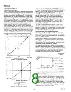
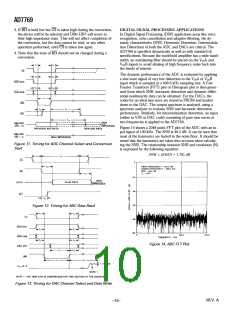
Figure 10. Negative-Going Settling Tim e
Inter nal / Exter nal Clock O per ation
T he AD7769 can be operated on either its own internal clock or
with an externally applied clock signal. For internal clock opera-
tion the CLK input must be tied to VDD. No external compo-
nents are required. T he internal clock typically runs at 5 MHz
giving a typical conversion time of 2.5 µs. For external clock op-
eration the CLK input must be driven with a T T L/ HCMOS
compatible input. T he mark/space ratio of the clock signal can
vary from 30/70 to 70/30. For an input frequency of 5 MHz, the
conversion time is 2.5 µs.
Tr ack-and-H old
T he track-and-hold (T /H) amplifier on the analog input to the
ADC of the AD7769 allows the ADC to accurately convert an
input sine wave of 5 V peak-to-peak amplitude up to a fre-
quency of 200 kHz, the Nyquist frequency of the ADC when
operated at its maximum throughput rate of 400 kHz. T his
maximum rate of conversion includes conversion time and time
between conversions. Because the input bandwidth of the track-
and-hold is much greater than 200 kHz, the input signal should
be band limited to avoid folding unwanted signals into the band
of interest.
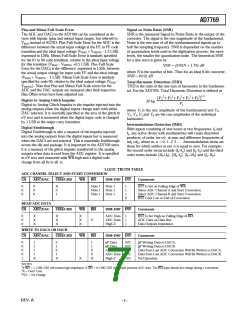
D igital Inputs and O utputs
T he AD7769 communicates over a standard, 8-bit microproces-
sor data bus and is controlled by standard mpu control lines,
CS, WR, RD, INT, plus two address lines, ADC/DAC and
CHA/CHB, which select the DAC or ADC function and Chan-
nel A or Channel B input/output channel. T he Chip Select (CS)
line selects the device, Write (WR) is used to initiate ADC con-
versions or to write data to the DAC, depending on the state of
ADC/DAC. INT is a status flag that indicates completion of a
conversion, while RD is used to read ADC output data. T he
8-bit data port (DB0–DB7) is a bidirectional port into which
data can be written to the two DAC registers, and from which
data can be read from the ADC register. ADC output data may
also be written directly into either of the DAC registers.
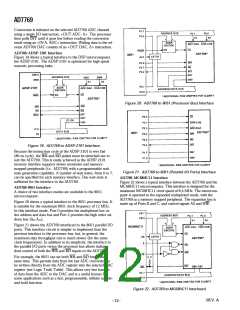
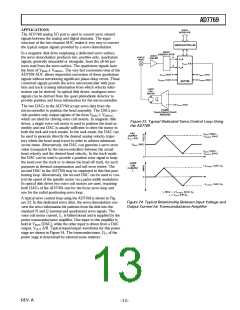
D AC O utputs
T he D/A converter outputs are buffered with on-board, high
speed op amps that are capable of driving 5 kΩ and 100 pF
loads to AGND (DAC). Each output amplifier settles to within
1/2 LSB of its final output value in typically less than 2.5 µs.
See Figures 9 and 10 for waveforms of the typical output set-
tling time performance.
T he output noise from the amplifiers with full scale on the
DACs is typically 200 µV peak-to-peak.
T hese logical operations are detailed in T able I and in the time
ing diagrams, Figures 11 to 13. Figures 12 and 13 show the
fairly straightforward operations of reading ADC data and writ-
ing data to the DACs, and need little explanation. Figure 11
shows the timing for ADC channel selection and conversion
start. T his is more complicated as the state of the data outputs
during a conversion depends on CS and RD.
T o initiate a conversion (or any other operation) the device
must be selected by taking CS low. A conversion is started by
taking WR low, then high again (conversion starts on rising edge
of WR). T here are three possibilities for the state of the data
outputs during the conversion.
1. If RD is held high, the data outputs will be high impedance
throughout the conversion.
2. If RD and CS are both held low until after INT goes low,
then DB0–DB7 will initially output data from the last con-
version. After INT goes low the new conversion data will
appear on DB0–DB7.
Figure 9. Positive-Going Settling Tim e
REV. A
–9–

 ADI [ ADI ]