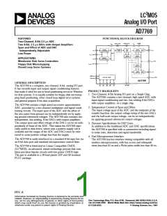
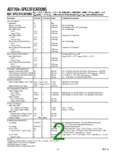
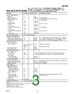
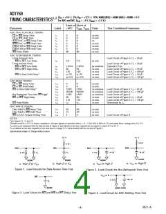
AD7769
ABSO LUTE MAXIMUM RATINGS*
Power Dissipation (Any Package)
VDD to AGND or DGND . . . . . . . . . . . . . . . . . –0.3 V, +15 V
VCC to DGND . . . . . . . . . . . . . . . . –0.3 V, VDD +0.3 V or 7 V
(Whichever is Lower)
AGND to DGND . . . . . . . . . . . . . . . . . . –0.3 V, VDD +0.3 V
Digital Inputs to DGND
to +75°C . . . . . . . . . . . . . . . . . . . . . . . . . . . . . . . . 500 mW
Derates Above +75°C by . . . . . . . . . . . . . . . . . . . 6 mW/°C
Storage T emperature Range . . . . . . . . . . . . –65°C to +150°C
Lead T emperature (Soldering 10 secs) . . . . . . . . . . . . +300°C
*Stresses above those listed under Absolute Maximum Ratings may cause perma-
nent damage to the device. T his is a stress rating only; functional operation of the
device at these or any other conditions above those listed in the operational
sections of this specification is not implied. Exposure to absolute maximum rating
conditions for extended periods may affect device reliability. Only one Absolute
Maximum Rating may be applied at any one time.
(Pins 12, 13, 15–18) . . . . . . . . . . . . . . –0.3 V, VDD +0.3 V
Digital Outputs to DGND
(Pins 3–10, 11) . . . . . . . . . . . . . . . . . . . –0.3 V, VCC +0.3 V
Analog Inputs to AGND . . . . . . . . . . . . . –0.3 V, VDD +0.3 V
Analog Outputs to AGND . . . . . . . . . . . . –0.3 V, VDD +0.3 V
Operating T emperature Range
Commercial (J Version) . . . . . . . . . . . . . . . . . 0°C to +70°C
Industrial (A Version) . . . . . . . . . . . . . . . . –40°C to +85°C
CAUTIO N
ESD (electrostatic discharge) sensitive device. Electrostatic charges as high as 4000 V readily
accumulate on the human body and test equipment and can discharge without detection.
Although the AD7769 features proprietary ESD protection circuitry, permanent damage may
occur on devices subjected to high energy electrostatic discharges. T herefore, proper ESD
precautions are recommended to avoid performance degradation or loss of functionality.
WARNING!
ESD SENSITIVE DEVICE
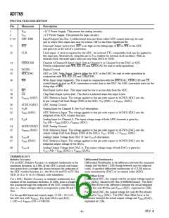
NOT E
O RD ERING GUID E
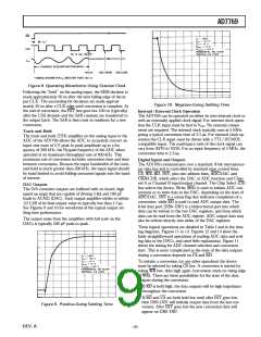
Do not allow VCC to exceed VDD by more than 0.3 V. In cases
where this can happen the diode protection scheme shown
below is recommended.
Tem perature
Range
P ackage
O ption*
Model
AD7769JN
AD7769JP
AD7769AN
AD7769AP
0°C to +70°C
0°C to +70°C
–40°C to +85°C
–40°C to +85°C
N-28
P-28A
N-28
P-28A
*N = Plastic DIP; P = Plastic Leaded Chip Carrier.
P IN CO NFIGURATIO NS
D IP
P LCC
REV. A
–5–

 ADI [ ADI ]