AD7769
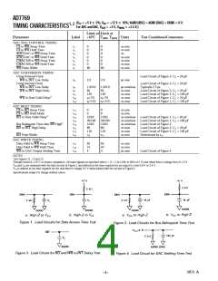
TIMING CHARACTERISTICS
(V = +5 V ؎ 5%; V = +12 V ؎ 10%; AGND [ADC] = AGND [DAC] = DGND = 0 V.
For ADC and DAC, VBIAS = +5 V, VSWING = +2.5 V.)
CC
DD
1, 2
Lim it at Lim it at
P aram eter
Label
+25؇C
TMIN, TMAX Units
Test Conditions/Com m ents
ADC /DAC CONT ROL T IMING
CS to WR Setup T ime
CS to WR Hold T ime
ADC/DAC to WR Setup T ime
ADC/DAC to WR Hold T ime
CHA/CHB to WR Setup T ime
CHA/CHB to WR Hold T ime
WR Pulse Width
t1
t2
t3
t4
t5
t6
t7
0
0
0
0
0
0
80
0
0
0
0
0
0
80
ns min
ns min
ns
ns min
ns min
ns min
ns min
ADC CONVERSION T IMING
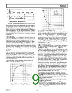
Using External Clock
Load Circuit of Figure 3, CL = 20 pF
WR to INT Low Delay
Using Internal Clock
WR to INT Low Delay
WR to INT High Delay
t8
2.6
2.6
µs max
Load Circuit of Figure 3, CL = 20 pF
T ypically 2.5 µs
Load Circuit of Figure 3, CL = 20 pF
Load Circuit of Figure 3, CL = 100 pF
Load Circuit of Figure 1, CL = 20 pF
Load Circuit of Figure 1, CL = 100 pF
t8
t9
t9
t10
t10
1.9/3.0
85
120
t8+70
t8+110
1.9/3.0
85
120
t8+70
t8+110
µs min/max
ns max
ns max
ns max
ns max
WR to Data Valid Delay3
ADC READ T IMING
CS to RD Setup T ime
CS to RD Hold Mode
RD to Data Valid Delay3
t11
t12
t13
t13
t14
t15
t15
t16
0
0
0
0
ns min
ns min
ns min/max
ns min/max
ns min/max
ns max
15/65
30/100
15/65
80
110
t13
15/65
30/100
15/65
80
110
t13
Load Circuit of Figure 1, CL = 20 pF
Load Circuit of Figure 1, C L = 100 pF
Load Circuit of Figure 2
Load Circuit of Figure 3, CL = 20 pF
Load Circuit of Figure 3, CL = 100 pF
Determined by t13
Bus Relinquish T ime after RD High4
RD to INT High Delay
ns max
ns min
RD Pulse Width
DAC WRIT E T IMING
Data Valid to WR Setup T ime
Data Valid to WR Hold T ime
WR to DAC Output Settling T ime
t17
t18
t19
65
15
4
65
20
4
ns nıin
ns min
µs max
Load Circuit of Figure 4
NOT ES
1See Figures 11, 12 and 13.
2Sample tested at +25°C to ensure compliance. All input signals are specified with tr = tf = 5 ns (10% to 90% of 5 V) and timed from a voltage level of 1.6 V.
3t10 and t13 are measured with the load circuits of Figure 1 and defined as the time required for an output to cross 0.8 V or 2.4 V.
4t14 is defined as the time required for the data lines to change 0.5 V when loaded with the circuits of Figure 2.
Specifications subject to change without notice.
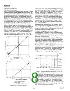
Figure 1. Load Circuits for Data Access Tim e Test
Figure 2. Load Circuits for Bus Relinquish Tim e Test
Figure 3. Load Circuit for RD and WR to INT Delay Test
Figure 4. Load Circuit for DAC Settling Tim e Test
REV. A
–4–

 ADI [ ADI ]