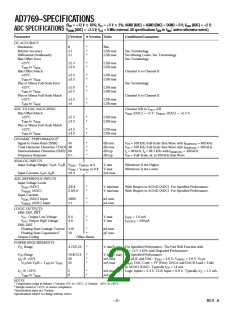
AD7769–SPECIFICATIONS
BIAS [ADC] = +5 V;
ADC SPECIFICATIONS (VV = +12 V ؎ 10%; V = +5 V ؎ 5%; AGND [ADC] = AGND [DAC] = DGND = 0 V; V
DD
CC
SWING [ADC] = +2.5 V; fCLK = 5 MHz external. All specifications TMIN to T 1 unless otherwise noted.)
MAX
P aram eter
J Version A Version Units
Conditions/Com m ents
DC ACCURACY
Resolution
Relative Accuracy
Differential Nonlinearity
Bias Offset Error
+25°C
8
±1
±1
*
*
*
Bits
LSB max
LSB max
See T erminology
No Missing Codes. See T erminology.
See T erminology
±2.5
±3.0
*
*
LSB max
LSB max
T MIN to T MAX
Bias Offset Match
+25°C
T MIN to T MAX
Plus or Minus Full-Scale Error
+25°C
T MIN to T MAX
Channel A to Channel B
See T erminology
±2.5
±3.5
*
*
LSB max
LSB max
±2.0
±2.5
*
*
LSB max
LSB max
Plus or Minus Full-Scale Match
+25°C
T MIN to T MAX
Channel A to Channel B
±3.5
±4
*
*
LSB max
LSB max
ADC T O DAC MAT CHING
Bias Offset Match
+25°C
Channel A/B to VOUT A/B
VBIAS (DAC) = +5 V, VSWING (DAC) = +2.5 V.
±2.5
±3.5
*
*
LSB max
LSB max
T MIN to T MAX
Plus or Minus Full-Scale Match
+25°C
T MIN to T MAX
±3.5
±4.0
*
*
LSB max
LSB max
DYNAMIC PERFORMANCE2
Signal-to-Noise Ratio (SNR)
T otal Harmonic Distortion (T HD) 48
Intermodulation Distortion (IMD) 60
44
*
*
*
*
dB min
dB max
dB typ
dB typ
VIN = 100 kHz Full-Scale Sine Wave with fSAMPLING = 400 kHz
VIN = 100 kHz Full-Scale Sine Wave with fSAMPLlNG = 400 kHz
fa = 99 kHz, fb = 96.7 kHz with fSAMPLING = 400 kHz
VIN = Full-Scale, dc to 200 kHz Sine Wave
Frequency Response
0.1
ANALOG INPUT S
Input Voltage Ranges, VINA, VIN
B
VBIAS – VSWING or 0
VBIAS + VSWING or 9.8
V min
V max
mA max
Whichever Is the Higher
Whichever Is the Lower
Input Currents, IINA, IIN
B
±0.4
*
ADC REFERENCE INPUT S
Input Voltage Levels
VBIAS (ADC)
2/6.8
2.0/3.0
*
*
V min/max
V min/max
With Respect to AGND (ADC). For Specified Performance.
With Respect to AGND (ADC). For Specified Performance.
VSWING (ADC)
Input Currents
VBIAS (ADC) Input
VSWING (ADC) Input
±800
±1
*
*
µA max
µA max
LOGIC OUT PUT S
DB0–DB7, INT
VOL, Output Low Voltage
0.4
4.0
*
*
V max
V min
ISINK = 1.6 mA
ISOURCE = 200 µA
VOH , Output High Voltage
DB0–DB7
Floating State Leakage Current ±10
*
*
µA max
pF max
Floating State Capacitance2
Output Coding
10
Offset Binary
POWER REQUIREMENT S
VCC Range
4.75/5.25
*
V min/V max For Specified Performance. T he Part Will Function with
VCC =5 V ±10% with Degraded Performance.
VDD Range
IDD @ +25°C
10.8/13.2
20
22
*
*
*
V min/V max For Specified Performance
mA max
mA max
For ADC and DAC: VBIAS = 5.0 V; VSWING = 3.0 V; VINA,
VBIAS; DAC Code = FF (Hex); DACA and DACB Load = 5 kΩ
to AGND (DAC). T ypically IDD = 14 mA.
VUBAm VINB = T MIN to T MAX
ICC @ +25°C
T MIN to T MAX
5
6
*
*
mA max
mA max
Logic Inputs = 2.4 V, CLK Input = 0.8 V. T ypically ICC = 1.5 mA.
NOT ES
1 T emperature range as follows: J Version: 0°C to +70°C; A Version: –40°C to +85°C.
2 Sample tested at +25°C to ensure compliance.
*Specification same as J Version.
Specifications subject to change without notice.
–2–
REV. A

 ADI [ ADI ]