AD73360L
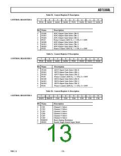
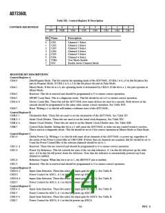
Table XII. Control Register H Description
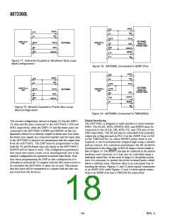
CONTROL REGISTER H
7
6
5
4
3
2
1
0
INV
TME
CH6
CH5
CH4
CH3
CH2
CH1
Bit Name
Description
0
1
2
3
4
5
6
7
CH1
CH2
CH3
CH4
CH5
CH6
TME
INV
Channel 1 Select
Channel 2 Select
Channel 3 Select
Channel 4 Select
Channel 5 Select
Channel 6 Select
Test Mode Enable
Enable Invert Channel Mode
REGISTER BIT DESCRIPTIONS
Control Register A
CRA:0
Data/Program Mode. This bit controls the operating mode of the AD73360L. If CRA:1 is 0, a 0 in this bit places the
part in Program Mode. If CRA:1 is 0, a 1 in this bit places the part in Data Mode.
CRA:1
Mixed Mode. If this bit is a 0, the operating mode is determined by CRA:0. If this bit is a 1, the part operates in
Mixed Mode.
CRA:2
Reserved. This bit is reserved and should be programmed to 0 to ensure correct operation.
CRA:3
SPORT Loop Back. This is a diagnostic mode. This bit should be set to 0 to ensure correct operation.
CRA:4–6
Device Count Bits. These bits tell the AD73360L how many devices are used in a cascade. Both devices in the
cascade should be programmed to the same value ensure correct operation. See Table XVI.
CRA:7
Reset. Writing a 1 to this bit will initiate a software reset of the AD73360L.
Control Register B
CRB:0–1
CRB:2–3
CRB:4–6
CRB:7
Decimation Rate. These bits are used to set the decimation of the AD73360L. See Table XV.
Serial Clock Divider. These bits are used to set the serial clock frequency. See Table XIV.
Master Clock Divider. These bits are used to set the Master Clock Divider ratio. See Table XIII.
Control Echo Enable. Setting this bit to a 1 will cause the AD73360L to write out any control words it receives.
This is used as a diagnostic mode. This bit should be set to 0 for correct operation in Mixed Mode or Data Mode.
Control Register C
CRC:0
Global Power-Up. Writing a 1 to this bit will cause all six channels of the AD73360L to power up, regardless of
the status of the Power Control Bits in CRD-CRF. If fewer than six channels are required, this bit should be set to
0 and the Power Control Bits of the relevant channels should be set to 1.
CRC:1–4
Reserved. These bits are reserved and should be programmed to 0 to ensure correct operation.
CRC:5
Power-Up Reference. This bit controls the state of the on-chip reference. A 1 in this bit will power up the refer-
ence. A 0 in this bit will power down the reference. Note that the reference is automatically powered up if any
channel is enabled.
CRC:6
CRC:7
Reference Output. When this bit is set to 1, the REFOUT pin is enabled.
Reserved. This bit is reserved and should be programmed to 0 to ensure correct operation.
Control Register D
CRD:0–2
Input Gain Selection. These bits select the input gain for ADC1. See Table II.
CRD:3
Power Control for ADC1. A 1 in this bit powers up ADC1.
CRD:4–6
CRD:7
Input Gain Selection. These bits select the input gain for ADC2. See Table II.
Power Control for ADC2. A 1 in this bit powers up ADC2.
Control Register E
CRE:0–2
Input Gain Selection. These bits select the input gain for ADC3. See Table II.
CRE:3
Power Control for ADC3. A 1 in this bit powers up ADC3.
CRE:4–6
CRE:7
Input Gain Selection. These bits select the input gain for ADC4. See Table II.
Power Control for ADC4. A 1 in this bit powers up ADC4.
–14–
REV. 0

 ADI [ ADI ]