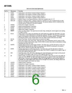
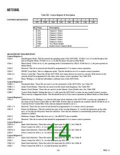
AD73360L
Voltage Reference
Note: As each AD73360L has its own SPORT section, the
register settings in all SPORTs must be programmed. The regis-
ters that control SPORT and sample rate operation (CRA and
CRB) must be programmed with the same values, otherwise
incorrect operation may occur.
The AD73360L reference, REFCAP, is a bandgap reference
that provides a low noise, temperature-compensated reference
to the ADC. A buffered version of the reference is also made
available on the REFOUT pin and can be used to bias other
external analog circuitry. The reference has a default nominal
value of 1.2 V.
In Program Mode (CRA:0 = 0), the device’s internal configura-
tion can be programmed by writing to the eight internal control
registers. In this mode, control information can be written to or
read from the AD73360L. In Data Mode (CRA:0 = 1), any infor-
mation that is sent to the device is ignored, while the encoder
section (ADC) data is read from the device. In this mode, only
ADC data is read from the device. Mixed mode (CRA:0 = 1 and
CRA:1 = 1) allows the user to send control information and
receive either control information or ADC data. This is achieved
by using the MSB of the 16-bit frame as a flag bit. Mixed mode
reduces the resolution to 15 bits with the MSB being used to
indicate whether the information in the 16-bit frame is control
information or ADC data.
The reference output (REFOUT) can be enabled for biasing
external circuitry by setting the RU bit (CRC:6) of CRC.
Serial Port (SPORT)
The AD73360Ls communicate with a host processor via the
bidirectional synchronous serial port (SPORT) which is compat-
ible with most modern DSPs. The SPORT is used to transmit
and receive digital data and control information. Two AD73360Ls
can be cascaded together to provide additional input channels.
In both transmit and receive modes, data is transferred at the
serial clock (SCLK) rate with the MSB being transferred first.
Due to the fact that the SPORT of each AD73360L block uses
a common serial register for serial input and output, communi-
cations between an AD73360L and a host processor (DSP
engine) must always be initiated by the AD73360Ls themselves.
In this configuration the AD73360Ls are described as being in
Master mode. This ensures that there is no collision between
input data and output samples.
The SPORT features a single 16-bit serial register that is used for
both input and output data transfers. As the input and output
data must share the same register, some precautions must be
observed. The primary precaution is that no information must be
written to the SPORT without reference to an output sample
event, which is when the serial register will be overwritten with
the latest ADC sample word. Once the SPORT starts to output
the latest ADC word, it is safe for the DSP to write new control
words to the AD73360L. In certain configurations, data can be
written to the device to coincide with the output sample being
shifted out of the serial register—see section on interfacing
devices. The serial clock rate (CRB:2–3) defines how many 16-bit
words can be written to a device before the next output sample
event will happen.
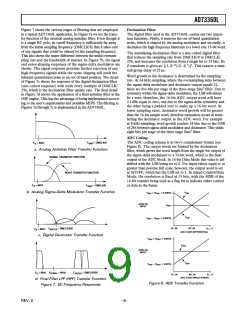
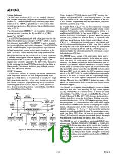
SPORT Overview
The AD73360L SPORT is a flexible, full-duplex, synchronous
serial port whose protocol has been designed to allow up to
eight AD73360L devices to be connected in cascade, to a single
DSP via a six-wire interface. It has a very flexible architecture
that can be configured by programming two of the internal
control registers in each device. The AD73360L SPORT has
three distinct modes of operation: Control Mode, Data Mode
and Mixed Control/Data Mode.
The SPORT block diagram, shown in Figure 9, details the blocks
associated with AD73360L including the eight control registers
(A–H), external MCLK to internal DMCLK divider and serial
clock divider. The divider rates are controlled by the setting of
Control Register B. The AD73360L features a master clock
divider that allows users the flexibility of dividing externally
available high-frequency DSP or CPU clocks to generate a lower
frequency master clock internally in the AD73360L which may be
more suitable for either serial transfer or sampling rate require-
ments. The master clock divider has five divider options (÷1
default condition, ÷2, ÷ 3, ÷ 4, ÷5) that are set by loading the
master clock divider field in Register B with the appropriate
code (see Table XIII). Once the internal device master clock
(DMCLK) has been set using the master clock divider, the sample
rate and serial clock settings are derived from DMCLK.
MCLK
DMCLK
(INTERNAL)
MCLK
DIVIDER
SCLK
SCLK
DIVIDER
SE
RESET
SDIFS
SDI
SERIAL PORT
(SPORT)
SDOFS
SDO
SERIAL REGISTER
2
3
8
8
8
8
8
CONTROL
REGISTER
A
CONTROL
REGISTER
B
CONTROL
REGISTER
C
CONTROL
REGISTER
D
CONTROL
REGISTER
E
The SPORT can work at four different serial clock (SCLK) rates:
chosen from DMCLK, DMCLK/2, DMCLK/4 or DMCLK/8,
where DMCLK is the internal or device master clock resulting
from the external or pin master clock being divided by the master
clock divider. Care should be taken when selecting Master Clock,
Serial Clock, and Sample Rate divider settings to ensure that
there is sufficient time to read all the data from the AD73360L
before the next sample interval.
CONTROL
REGISTER
F
CONTROL
REGISTER
G
CONTROL
REGISTER
H
8
Figure 9. SPORT Block Diagram
–10–
REV. 0

 ADI [ ADI ]