AD73360L
SDIFS
SDI
TFS
DT
SDIFS
SDI
TFS
DT
SCLK
SCLK
SDO
AD73360L
ANALOG
FRONT-END
ADSP-21xx
DSP
SCLK
SCLK
ADSP-21xx
DSP
AD73360L
DR
DR
SDO
RFS
SDOFS
RFS
SDOFS
RESET
FL0
FL1
SE
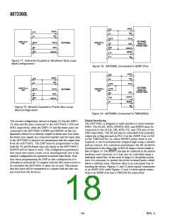
Figure 11. Indirectly Coupled or Nonframe Sync Loop-
Back Configuration
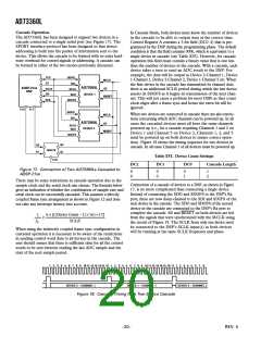
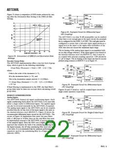
Figure 13. AD73360L Connected to ADSP-21xx
SDIFS
SDI
FSX
DX
SDIFS
TFS
SDI
DT
CLKX
SCLK
AD73360L
ANALOG
FRONT-END
ADSP-21xx
DSP
CLKR
DR
SCLK
SCLK
TMS320C5x
DSP
AD73360L
SDO
DR
SDO
SDOFS
FSR
XF
RFS
SDOFS
RESET
SE
Figure 12. Directly Coupled or Frame Sync Loop-
Back Configuration
Figure 14. AD73360L Connected to TMS320C5x
Digital Interfacing
The second configuration (shown in Figure 12) has the DSP’s
Tx data and Rx data connected to the AD73360L’s SDI and
SDO, respectively, while the DSP’s Tx and Rx frame syncs are
connected to the AD73360L’s SDIFS and SDOFS. In this con-
figuration, referred to as directly coupled or frame sync loop-back,
the frame sync signals are connected together and the input data
to the AD73360L is forced to be synchronous with the output data
from the AD73360L. The DSP must be programmed so that
both the Tx and Rx frame syncs are inputs as the AD73360L’s
SDOFS will be input to both. This configuration guarantees
that input and output events occur simultaneously and is the
simplest configuration for operation in normal Data Mode. Note
that when programming the DSP in this configuration it is
advisable to preload the Tx register with the first control word to
be sent before the AD73360L is taken out of reset. This ensures
that this word will be transmitted to coincide with the first out-
put word from the device(s).
The AD73360L is designed to easily interface to most common
DSPs. The SCLK, SDO, SDOFS, SDI, and SDIFS must be
connected to the SCLK, DR, RFS, DT, and TFS pins of the
DSP respectively. The SE pin may be controlled from a parallel
output pin or flag pin such as FL0–2 on the ADSP-21xx (or XF
on the TMS320C5x) or, where SPORT power-down is not
required, it can be permanently strapped high using a suitable
pull-up resistor. For consistent performance the SE should be
synchronized to the rising edge of MCLK using a circuit similar to
that of Figure 19. The RESET pin may be connected to the system
hardware reset structure or it may also be controlled using a
dedicated control line. In the event of tying it to the global system
reset, it is necessary to operate the device in mixed mode, which
allows a software reset, otherwise there is no convenient way of
resetting the device. Figures 11 and 12 show typical connections
to an ADSP-2181 while Figures 13 and 14 show typical connec-
tions to an ADSP-21xx and a TMS320C5x, respectively.
–18–
REV. 0

 ADI [ ADI ]