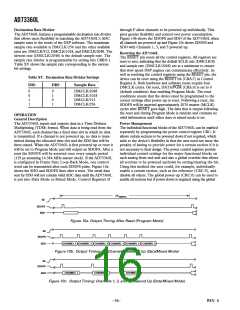
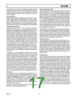
AD73360L
Decimation Rate Divider
through F allow channels to be powered up individually. This
gives greater flexibility and control over power consumption.
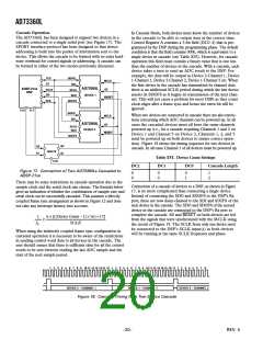
Figure 10b shows the SDOFS and SDO of the AD73360L when
all channels are powered up and Figure 10c shows SDOFS and
SDO with Channels 1, 3, and 5 powered up.
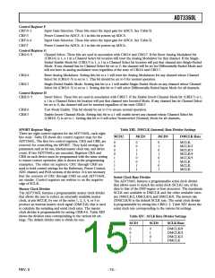
The AD73360L features a programmable decimation rate divider
that allows users flexibility in matching the AD73360L’s ADC
sample rates to the needs of the DSP software. The maximum
sample rate available is DMCLK/256 and the other available
rates are: DMCLK/512, DMCLK/1024, and DMCLK/2048. The
slowest rate (DMCLK/2048) is the default sample rate. The
sample rate divider is programmable by setting bits CRB:0-1.
Table XV shows the sample rate corresponding to the various
bit settings.
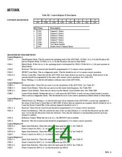
Resetting the AD73360L
The RESET pin resets all the control registers. All registers are
reset to zero, indicating that the default SCLK rate (DMCLK/8)
and sample rate (DMCLK/2048) are at a minimum to ensure
that slow speed DSP engines can communicate effectively. As
well as resetting the control registers using the RESET pin, the
device can be reset using the RESET bit (CRA:7) in Control
Register A. Both hardware and software resets require four
DMCLK cycles. On reset, DATA/PGM (CRA:0) is set to 0
(default condition) thus enabling Program Mode. The reset
conditions ensure that the device must be programmed to the
correct settings after power-up or reset. Following a reset, the
SDOFS will be asserted approximately 2070 master (MCLK)
cycles after RESET goes high. The data that is output following
the reset and during Program Mode is random and contains no
valid information until either data or mixed mode is set.
Table XV. Decimation Rate Divider Settings
DR1
DR0
Sample Rate
0
0
1
1
0
1
0
1
DMCLK/2048
DMCLK/1024
DMCLK/512
DMCLK/256
OPERATION
General Description
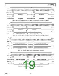
The AD73360L inputs and outputs data in a Time Division
Multiplexing (TDM) format. When data is being read from the
AD73360L each channel has a fixed time slot in which its data
is transmitted. If a channel is not powered up, no data is trans-
mitted during the allocated time slot and the SDO line will be
three-stated. When the AD73360L is first powered up or reset it
will be set to Program Mode and will output an SDOFS. After a
reset the SDOFS will be asserted once every sample period
(125 µs assuming 16.384 MHz master clock). If the AD73360L
is configured in Frame Sync Loop-Back Mode, one control
word can be transmitted after each SDOFS pulse. Figure 10a
shows the SDO and SDOFS lines after a reset. The serial data
sent by SDO will not contain valid ADC data until the AD73360L
is put into Data Mode or Mixed Mode. Control Registers D
Power Management
The individual functional blocks of the AD73360L can be enabled
separately by programming the power control register CRC. It
allows certain sections to be powered down if not required, which
adds to the device’s flexibility in that the user need not incur the
penalty of having to provide power for a certain section if it is
not necessary to their design. The power control registers provide
individual control settings for the major functional blocks on
each analog front-end unit and also a global override that allows
all sections to be powered up/down by setting/clearing the bit.
Using this method the user could, for example, individually
enable a certain section, such as the reference (CRC:5), and
disable all others. The global power-up (CRC:0) can be used to
enable all sections but if power-down is required using the global
1/F
SAMPLE
SE
SDOFS
SDO
Figure 10a. Output Timing After Reset (Program Mode)
SE
SDOFS
SDO
CHANNEL 1 CHANNEL 2 CHANNEL 3 CHANNEL 4 CHANNEL 5 CHANNEL 6
Figure 10b. Output Timing: All Channels Powered Up (Data/Mixed Mode)
SE
SDOFS
CHANNEL 1
CHANNEL 5
CHANNEL 3
SDO
Figure 10c. Output Timing: Channels 1, 3, and 5 Powered Up (Data/Mixed Mode)
–16–
REV. 0

 ADI [ ADI ]