AD73360L
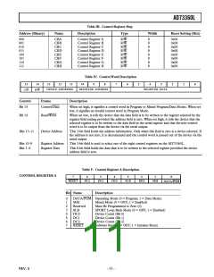
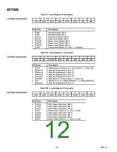
Table VI. Control Register B Description
CONTROL REGISTER B
7
6
5
4
3
2
1
0
CEE
MCD2
MCD1
MCD0
SCD1
SCD0
DR1
DR0
Bit Name
Description
0
1
2
3
4
5
6
7
DR0
DR1
Decimation Rate (Bit 0)
Decimation Rate (Bit 1)
Serial Clock Divider (Bit 0)
Serial Clock Divider (Bit 1)
Master Clock Divider (Bit 0)
Master Clock Divider (Bit 1)
Master Clock Divider (Bit 2)
SCD0
SCD1
MCD0
MCD1
MCD2
CEE
Control Echo Enable (0 = OFF; 1 = Enabled)
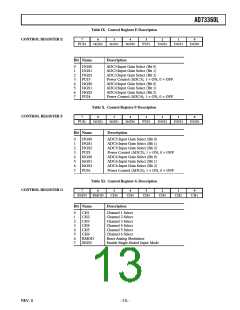
Table VII. Control Register C Description
CONTROL REGISTER C
7
6
5
4
3
2
1
0
RES
RU
PUREF
RES
RES
RES
RES
GPU
Bit Name
Description
0
1
2
3
4
5
6
7
GPU
Global Power-Up Device (0 = Power Down; 1 = Power Up)
Must Be Programmed to Zero (0)
Must Be Programmed to Zero (0)
Must Be Programmed to Zero (0)
Must Be Programmed to Zero (0)
REF Power (0 = Power Down; 1 = Power Up)
REFOUT Use (0 = Disable REFOUT; 1 = Enable REFOUT)
Must Be Programmed to Zero (0)
Reserved
Reserved
Reserved
Reserved
PUREF
RU
Reserved
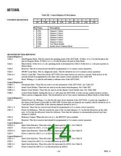
Table VIII. Control Register D Description
CONTROL REGISTER D
7
6
5
4
3
2
1
0
PUI2
I2GS2
I2GS1
I2GS0
PUI1
I1GS2
I1GS1
I1GS0
Bit Name
Description
0
1
2
3
4
5
6
7
I1GS0
I1GS1
I1GS2
PUI1
I2GS0
I2GS1
I2GS2
PUI2
ADC1:Input Gain Select (Bit 0)
ADC1:Input Gain Select (Bit 1)
ADC1:Input Gain Select (Bit 2)
Power Control (ADC1); 1 = ON, 0 = OFF
ADC2:Input Gain Select (Bit 0)
ADC2:Input Gain Select (Bit 1)
ADC2:Input Gain Select (Bit 2)
Power Control (ADC2); 1 = ON, 0 = OFF
–12–
REV. 0

 ADI [ ADI ]