AD652
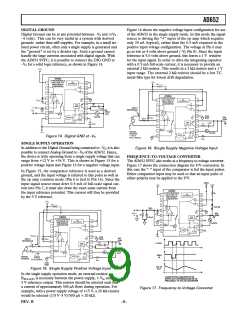
DIGITAL GROUND
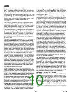
Figure 16 shows the negative voltage input configuration for use
of the AD652 in the single supply mode. In this mode the signal
source is driving the “+” input of the op amp which requires
only 20 nA (typical), rather than the 0.5 mA required in the
positive input voltage configuration. The voltage at Pin 6 may
go as low as 4 volts above ground (–VS Pin 8). Since the input
reference is 5.0 volts above ground, this leaves a 1 V window
for the input signal. In order to drive the integrating capacitor
with a 0.5 mA full-scale current, it is necessary to provide an
external 2 kΩ resistor. This results in a 2 kΩ resistor and a 1 V
input range. The external 2 kΩ resistor should be a low TC
metal-film type for lowest drift degradation.
Digital Ground can be at any potential between –VS and (+VS
–4 volts). This can be very useful in a system with derived
grounds rather than stiff supplies. For example, in a small iso-
lated power circuit, often only a single supply is generated and
the “ground” is set by a divider tap. Such a ground cannot
handle the large currents associated with digital signals. With
the AD652 SVFC, it is possible to connect the DIG GND to
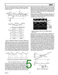
–VS for a solid logic reference, as shown in Figure 14.
Figure 14. Digital GND at –VS
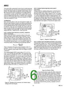
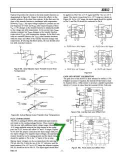
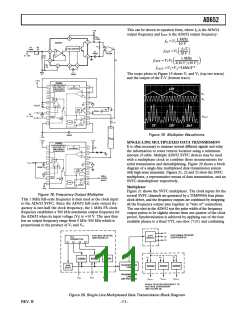
SINGLE SUPPLY OPERATION
In addition to the Digital Ground being connected to –VS, it is also
possible to connect Analog Ground to –VS of the AD652. Hence,
the device is truly operating from a single supply voltage that can
range from +12 V to +36 V. This is shown in Figure 15 for a
positive voltage input and Figure 16 for a negative voltage input.
Figure 16. Single Supply Negative Voltage Input
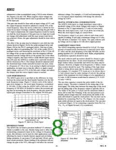
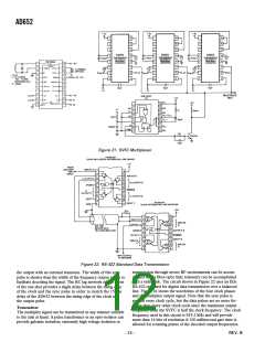
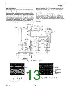
FREQUENCY-TO-VOLTAGE CONVERTER
The AD652 SVFC also works as a frequency-to-voltage converter.
Figure 17 shows the connection diagram for F/V conversion. In
this case the “–” input of the comparator is fed the input pulses.
Either comparator input may be used so that an input pulse of
either polarity may be applied to the F/V.
In Figure 15, the comparator reference is used as a derived
ground, and the input voltage is referred to this point as well as
the op amp common mode (Pin 6 is tied to Pin 16). Since the
input signal source must drive 0.5 mA of full-scale signal cur-
rent into Pin 7, it must also draw the exact same current from
the input reference potential. This current will thus be provided
by the 5 V reference.
Figure 15. Single Supply Positive Voltage Input
In the single supply operation mode, an external resistor,
RPULLUP, is necessary between the power supply, + VS, and the
5 V reference output. This resistor should be selected such that
a current of approximately 500 µA flows during operation. For
example, with a power supply voltage of +15 V, a 20 kΩ resistor
would be selected ((15 V–5 V)/500 µA = 20 kΩ).
Figure 17. Frequency-to-Voltage Converter
REV. B
–9–

 ADI [ ADI ]