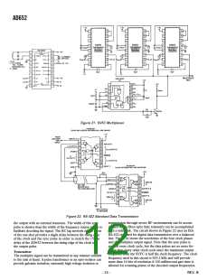
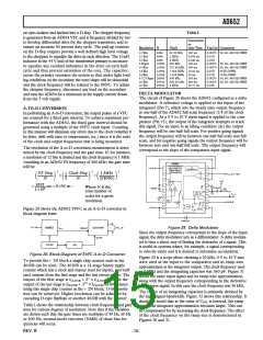
AD652
SVFC Demultiplexer
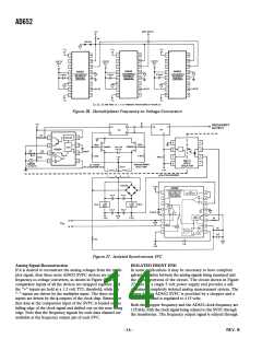
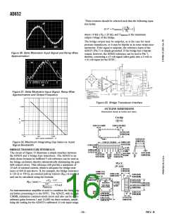
data pulse, then when the D-flop samples at the end of the one-
shot period, the signal will still be low and no pulse will appear
at the reconstructed clock output. These waveforms are shown
in Figure 25.
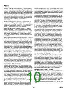
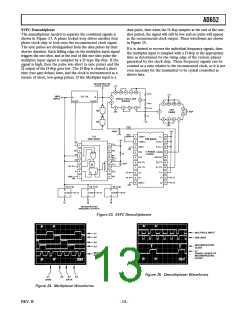
The demultiplexer needed to separate the combined signals is
shown in Figure 23. A phase locked loop drives another four
phase clock chip to lock onto the reconstructed clock signal.
The sync pulses are distinguished from the data pulses by their
shorter duration. Each falling edge on the multiplex input signal
triggers the one-shot, and at the end of this one-shot pulse the
multiplex input signal is sampled by a D-type flip-flop. If the
signal is high, then the pulse was short (a sync pulse) and the
Q output of the D-flop goes low. The D-flop is cleared a short
time (two gate delays) later, and the clock is reconstructed as a
stream of short, low-going pulses. If the Multiplex input is a
If it is desired to recover the individual frequency signals, then
the multiplex input is sampled with a D-flop at the appropriate
time as determined by the rising edge of the various phases
generated by the clock chip. These frequency signals can be
counted as a ratio relative to the reconstructed clock, so it is not
even necessary for the transmitter to be crystal controlled as
shown here.
Figure 23. SVFC Demultiplexers
Figure 25. Demultiplexer Waveforms
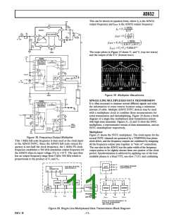
Figure 24. Multiplexer Waveforms
REV. B
–13–

 ADI [ ADI ]