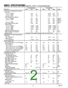
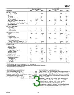
AD652
there are no problems with dielectric absorption causing the
duration of a reset pulse to be influenced by the length of time
since the last reset.
finally, a whole cycle is lost. When the cycle is lost, the Integrate
Phase lasts for two periods of the clock instead of the usual three
periods. Thus, among a long string of divide-by-fours an occasional
divide-by-three occurs; the average of the output frequency is
very close to one quarter of the clock, but the instantaneous fre-
quency can be very different.
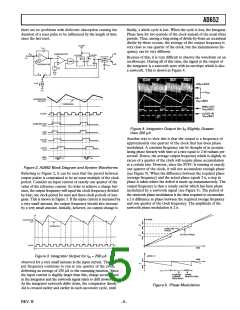
Because of this, it is very difficult to observe the waveform on an
oscilloscope. During all of this time, the signal at the output of
the integrator is a sawtooth wave with an envelope which is also
a sawtooth. This is shown in Figure 4.
Figure 4. Integrator Output for IIN Slightly Greater
than 250 µA
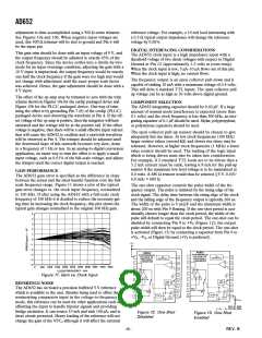
Another way to view this is that the output is a frequency of
approximately one quarter of the clock that has been phase
modulated. A constant frequency can be thought of as accumu-
lating phase linearly with time at a rate equal to 2 πf radians per
second. Hence, the average output frequency which is slightly in
excess of a quarter of the clock will require phase accumulation
at a certain rate. However, since the SVFC is running at exactly
one quarter of the clock, it will not accumulate enough phase
(see Figure 5). When the difference between the required phase
(average frequency) and the actual phase equals 2 π, a step in
phase is taken where the deficit is made up instantaneously. The
output frequency is then a steady carrier which has been phase
modulated by a sawtooth signal (see Figure 5). The period of
the sawtooth phase modulation is the time required to accumulate
a 2 π difference in phase between the required average frequency
and one quarter of the clock frequency. The amplitude of the
sawtooth phase modulation is 2 π.
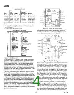
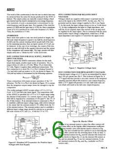
Figure 2. AD652 Block Diagram and System Waveforms
Referring to Figure 2, it can be seen that the period between
output pulses is constrained to be an exact multiple of the clock
period. Consider an input current of exactly one quarter of the
value of the reference current. In order to achieve a charge bal-
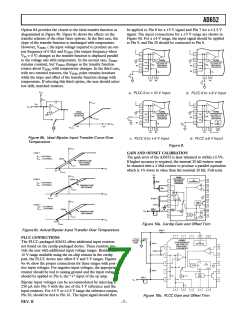
ance, the output frequency will equal the clock frequency divided
by four; one clock period for reset and three clock periods of inte-
grate. This is shown in Figure 3. If the input current is increased by
a very small amount, the output frequency should also increase
by a very small amount. Initially, however, no output change is
Figure 3. Integrator Output for lIN = 250 µA
observed for a very small increase in the input current. The out-
put frequency continues to run at one quarter of the clock,
delivering an average of 250 µA to the summing junction. Since
the input current is slightly larger than this, charge accumulates
in the integrator and the sawtooth signal starts to drift downward.
As the integrator sawtooth drifts down, the comparator thresh-
old is crossed earlier and earlier in each successive cycle, until
Figure 5. Phase Modulation
REV. B
–5–

 ADI [ ADI ]