AD652
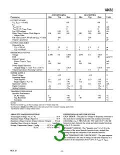
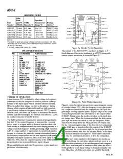
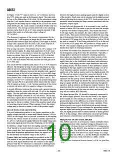
Option #4 provides the closest to the ideal transfer function as
diagrammed in Figure 8b. Figure 8c shows the effects on the
transfer relation of the other three options. In the first case, the
slope of the transfer function is unchanged with temperature.
However, VZERO ( the input voltage required to produce an out-
put frequency of 0 Hz) and FZERO (the output frequency when
VIN = 0 V) changes as the transfer function is displaced parallel
to the voltage axis with temperature. In the second case, FZERO
remains constant, but VZERO changes as the transfer function
rotates about FZERO with temperature changes. In the third case,
with two external resistors, the VZERO point remains invariant
while the slope and offset of the transfer function change with
temperature. If selecting this third option, the user should select
low drift, matched resistors.
be applied to Pin 8 for a 5 V signal and Pin 7 for a 2.5 V
signal. The input connections for a 5 V range are shown in
Figure 9d. For a 4 V range, the input signal should be applied
to Pin 9, and Pin 20 should be connected to Pin 8.
Figure 8b. Ideal Bipolar Input Transfer Curve Over
Temperature
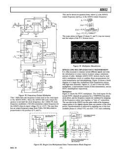
Figure 9.
GAIN AND OFFSET CALIBRATION
The gain error of the AD652 is laser trimmed to within 0.5%.
If higher accuracy is required, the internal 20 kΩ resistor must
be shunted with a 2 MΩ resistor to produce a parallel equivalent
which is 1% lower in value than the nominal 20 kΩ. Full-scale
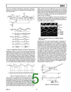
Figure 10a. Cerdip Gain and Offset Trim
Figure 8c. Actual Bipolar Input Transfer Over Temperature
PLCC CONNECTIONS
The PLCC packaged AD652 offers additional input resistors
not found on the cerdip-packaged device. These resistors pro-
vide the user with additional input voltage ranges. Besides the
10 V range available using the on-chip resistor in the cerdip
part, the PLCC device also offers 8 V and 5 V ranges. Figures
9a–9c show the proper connections for these ranges with posi-
tive input voltages. For negative input voltages, the appropriate
resistor should be tied to analog ground and the input voltage
should be applied to Pin 6, the “+” input of the op amp.
Bipolar input voltages can be accommodated by injecting a
250 µA into Pin 5 with the use of the 5 V reference and the
input resistors. For 5 V or 2.5 V range the reference output,
Pin 20, should be tied to Pin 10. The input signal should then
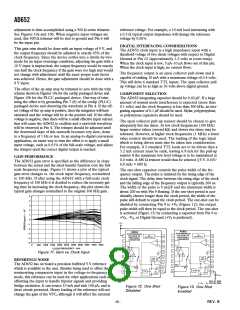
Figure 10b. PLCC Gain and Offset Trim
REV. B
–7–

 ADI [ ADI ]