AD652
The result of this synchronism is that the rate at which data may
be extracted from the series bit stream produced by the SVFC is
limited. The output pulses are typically counted during a fixed
gate interval and the result is interpreted as an average frequency.
The resolution of such a measurement is determined by the
clock frequency and the gate time. For example, if the clock fre-
quency is 4 MHz and the gate time is 4.096 ms, then a maximum
count of 8,192 is produced by a full-scale frequency of 2 MHz.
Thus, the resolution is 13 bits.
SVFC CONNECTIONS FOR NEGATIVE INPUT
VOLTAGES
Voltages which are negative with respect to ground may be
used as the input to the AD652 SVFC. In this case, Pin 7 is
grounded and the input voltage is applied to Pin 6 (see Figure
7). In this mode the input voltage can go as low as 4 volts above
–VS. In this configuration the input is a high impedance, and
only the 20 nA (typical) input bias current of the op amp need
be supplied by the input signal. This is contrasted with the more
usual positive input voltage configuration, which has a 20 kΩ
input impedance and requires 0.5 mA from the signal source.
OVERRANGE
Since each reset pulse is only one clock period in length, the
full-scale output frequency is equal to one-half the clock frequency.
At full scale the current steering switch spends half of the time
on the summing junction; thus, an input current of 0.5 mA can
be balanced. In the case of an overrange, the output of the inte-
grator op amp will drift in the negative direction and the output
of the comparator will remain high. The logic circuits will then
simply settle into a “divide-by-two” of the clock state.
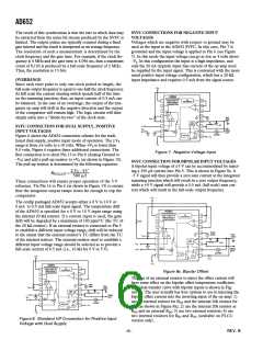
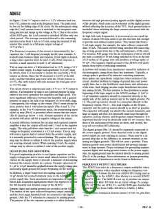
SVFC CONNECTION FOR DUAL SUPPLY, POSITIVE
INPUT VOLTAGES
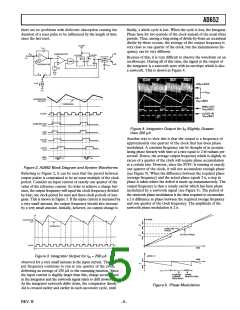
Figure 6 shows the AD652 connection scheme for the tradi-
tional dual supply, positive input mode of operation. The VS
range is from 6 volts to 18 volts. When +VS is lower than
9.0 volts, Figure 6 requires three additional connections. The
first connection is to short Pin 13 to Pin 8 (Analog Ground to
–VS) and add a pull-up resistor to +VS (as shown in Figure 15).
The pull-up resistor is determined by the following equation:
Figure 7. Negative Voltage Input
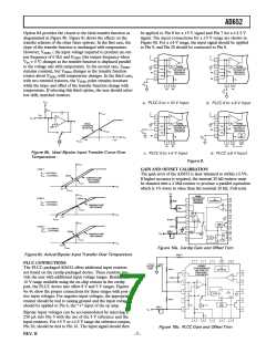
SVFC CONNECTION FOR BIPOLAR INPUT VOLTAGES
A bipolar input voltage of 5 V can be accommodated by inject-
ing a 250 µA current into Pin 5. This is shown in Figure 8a. A
–5 V signal will then provide a zero sum current at the integrator
summing junction which will result in a zero output frequency,
while a +5 V signal will provide a 0.5 mA (full-scale) sum cur-
rent which will result in the full-scale output frequency.
2VS – 5V
500 µA
RPULLUP
=
These connections will ensure proper operation of the 5 V
reference. Tie Pin 16 to Pin 6 (as shown in Figure 15) to ensure
that the integrator output ramps down far enough to trip the
comparator.
The cerdip packaged AD652 accepts either a 0 V to 10 V or
0 mA to 0.5 mA full-scale input signal. The temperature drift
of the AD652 is specified for a 0 V to 10 V input range using
the internal 20 kΩ resistor. If a current input is used, the gain
drift will be degraded by a maximum of 100 ppm/°C (the TC of
the 20 kΩ resistor). If an external resistor is connected to Pin 5
to establish a different input voltage range, drift will be induced
to the extent that the external resistor’s TC differs from the TC
of the internal resistor. The external resistor used to establish a
different input voltage range should be selected as to provide a
full-scale current of 0.5 mA (i.e., 10 kΩ for 0 V to 5 V).
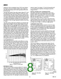
Figure 8a. Bipolar Offset
The use of an external resistor to inject the offset current will
have some effect on the bipolar offset temperature coefficient.
The ideal transfer curve with bipolar inputs is shown in Fig-
ure 8b. The user actually has four options to use in injecting the
bipolar offset current into the inverting input of the op amp: 1)
use an external resistor for ROS and the internal 20k resistor for
RIN (as shown in Figure 8a); 2) use the internal 20k resistor as
ROS and an external RIN; 3) use two external resistors; 4) use
two internal resistors for RIN and ROS (available on PLCC
version only).
Figure 6. Standard V/F Connection for Positive Input
Voltage with Dual Supply
–6–
REV. B

 ADI [ ADI ]