AD652
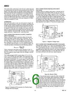
In Figure 17 the “+” input is tied to a 1.2 V reference and low
level TTL pulses are used as the frequency input. The pulse must
be low on the falling edge of the clock. On the subsequent rising
edge the 1 mA current source is switched to the integrator sum-
ming junction and ramps up the voltage at Pin 4. Due to the action
of the AND gate, the 1 mA current is switched off after only one
clock period. The average current delivered to the summing
junction varies from 0 mA to 0.5 mA; using the internal 20 kΩ
resistor this results in a full-scale output voltage of
between the high precision analog signals and the digital section
of the circuitry. Much noise can be tolerated on the digital ground
without affecting the accuracy of the VFC. Such ground noise is
inevitable when switching the large currents associated with the
frequency output signal.
At high full-scale frequencies, it is necessary to use a pull-up
resistor of about 500 Ω in order to get the rise time fast enough
to provide well defined output pulses. This means that from a
5 volt logic supply, for example, the open collector output will
draw 10 mA. This much current being switched will cause ring-
ing on long ground runs due to the self inductance of the wires.
For instance, #20 gauge wire has an inductance of about 20 nH
per inch; a current of 10 mA being switched in 50 ns at the end
of 12 inches of 20 gauge wire will produce a voltage spike of
50 mV. The separate digital ground of the AD652 will easily
handle these types of switching transients.
10 V at Pin 4.
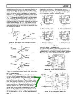
The frequency response of the circuit is determined by the
capacitor; the –3 dB frequency is simply the RC time constant. A
tradeoff exists between ripple and response. If low ripple is desired,
a large value capacitor must be used (1 µF), if fast response is
needed, a small capacitor is used (1 nF minimum).
The op amp can drive a 5 kΩ resistor load to 10 V, using a 15 V
positive power supply. If a large load capacitance (0.01 µF) must
be driven, then it is necessary to isolate the load with a 50 Ω
resistor as shown. Since the 50 Ω resistor is 0.25% of the full
scale, and the specified gain error with the 20 kΩ resistor is
0.5%, this extra resistor will only increase the total gain error
to +0.75% max.
A problem will remain from interference caused by radiation of
electromagnetic energy from these fast transients. Typically, a
voltage spike is produced by inductive switching transients;
these spikes can capacitively couple into other sections of the
circuit. Another problem is ringing of ground lines and power
supply lines due to the distributed capacitance and inductance
of the wires. Such ringing can also couple interference into sensi-
tive analog circuits. The best solution to these problems is proper
bypassing of the logic supply at the AD652 package. A 1 µF to
10 µF tantalum capacitor should be connected directly to the
supply side of the pull-up resistor and to the digital ground, Pin
12. The pull-up resistor should be connected directly to the
frequency output, Pin 11. The lead lengths on the bypass
capacitor and the pull-up resistor should be as short as possible.
The capacitor will supply (or absorb) the current transients, and
large ac signals will flow in a physically small loop through the
capacitor, pull-up resistor, and frequency output transistor. It is
important that the loop be physically small for two reasons: first,
there is less inductance if the wires are short, and second, the
loop will not radiate RFI efficiently.
The circuit shown is unipolar and only a 0 V to + 10 V output is
allowed. The integrator op amp is not a general purpose op amp,
rather it has been optimized for simplicity and high speed. The
most significant difference between this amplifier and a general
purpose op amp is the lack of an integrator (or level shift) stage.
Consequently, the voltage on the output (Pin 4) must always be
more positive than 1 volt below the inputs (Pins 6 and 7). For
example, in the F-to-V conversion mode, the noninverting input
of the op amp (Pin 6) is grounded which means that the output
(Pin 4) cannot go below –1 volt. Normal operation of the circuit
as shown will never call for a negative voltage at the output.
A second difference between this op amp and a general purpose
amplifier is that the output will only sink 1.5 mA to the negative
supply. The only pull-down other than the 1 mA current used for
voltage-to-frequency conversion is a 0.5 mA source. The op amp
will source a great deal of current from the positive supply, and
it is internally protected by current limiting. The output of the op
amp may be driven to within 4 volts of the positive supply when
not sourcing external current. When sourcing 10 mA, the output
voltage may be driven to within 6 volts of the positive supply.
The digital ground (Pin 12) should be separately connected to
the power supply ground. Note that the leads to the digital
power supply are only carrying dc current. There may be a dc
ground drop due to the difference in currents returned on the
analog and digital grounds. This will not cause a problem. These
features greatly ease power distribution and ground manage-
ment in large systems. Proper technique for grounding requires
separate digital and analog ground returns to the power supply.
Also, the signal ground must be referred directly to analog ground
(Pin 6) at the package. More information on proper grounding
and reduction of interference can be found in Reference 1.
DECOUPLING AND GROUNDING
It is good engineering practice to use bypass capacitors on the
supply-voltage pins and to insert small valued resistors (10 Ω to
100 Ω) in the supply lines to provide a measure of decoupling
between the various circuits in a system. Ceramic capacitors of
0.1 µF to 1.0 µF should be applied between the supply voltage pins
and analog signal ground for proper bypassing on the AD652.
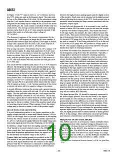
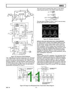
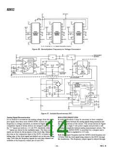
FREQUENCY OUTPUT MULTIPLIER
The AD652 can serve as a frequency output multiplier when
used in conjunction with a standard voltage-to-frequency con-
verter. Figure 18 shows the low cost AD654 VFC being used as
the clock input to the AD652. Also shown is a second AD652
in the F/V mode. The AD654 is set up to produce an output
frequency of 0 kHz–500 kHz for an input voltage (V1) range
of 0 V–10 V. The use of R4, C1, and the XOR gate doubles this
output frequency from 0 kHz–500 kHz to 0 MHz–1 MHz.
In addition, a larger board level decoupling capacitor of 1 µF to
10 µF should be located relatively close to the AD652 on each
power supply line. Such precautions are imperative in high reso-
lution data acquisition applications where one expects to exploit
the full linearity and dynamic range of the AD652.
Separate digital and analog grounds are provided on the AD652.
The emitter of the open collector frequency output transistor
and the clock input threshold only are returned to the digital
ground. Only the 5 V reference is connected to analog ground.
The purpose of the two separate grounds is to allow isolation
1“Noise Reduction Techniques in Electronic Systems,” by H.W. Ort, (John Wiley,
1976).
–10–
REV. B

 ADI [ ADI ]