AD652
This can be shown in equation form, where fC is the AD654
output frequency and fOUT is the AD652 output frequency:
1 MHz
10V
fC = V1
fC/2
10V
fOUT = V
2
1 MHz
2(10 V )(10V )
fOUT = V1V
2
fOUT =V1 •V2 •5kHz/V 2
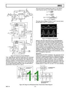
The scope photo in Figure 19 shows V1 and V2 (top two traces)
and the output of the F-V (bottom trace).
Figure 19. Multiplier Waveforms
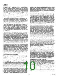
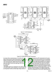
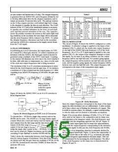
SINGLE-LINE MULTIPLEXED DATA TRANSMISSION
It is often necessary to measure several different signals and relay
the information to some remote location using a minimum
amount of cable. Multiple AD652 SVFC devices may be used
with a multiphase clock to combine these measurements for
serial transmission and demultiplexing. Figure 20 shows a block
diagram of a single-line multiplexed data transmission system
with high noise immunity. Figures 21, 22 and 23 show the SVFC
multiplexer, a representative means of data transmission, and an
SVFC demultiplexer respectively.
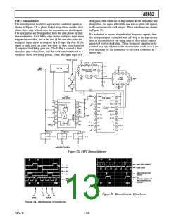
Multiplexer
Figure 21 shows the SVFC multiplexer. The clock inputs for the
several SVFC channels are generated by a TIM9904A four phase
clock driver, and the frequency outputs are combined by strapping
all the frequency output pins together (a “wire or” connection).
The one-shot in the AD652 sets the pulse width of the frequency
output pulses to be slightly shorter than one quarter of the clock
period. Synchronization is achieved by applying one of the four
available phases to a fixed TTL one-shot (’121) and combining
Figure 18. Frequency Output Multiplier
This 1 MHz full-scale frequency is then used as the clock input
to the AD652 SVFC. Since the AD652 full-scale output fre-
quency is one-half the clock frequency, the 1 MHz FS clock
frequency establishes a 500 kHz maximum output frequency for
the AD652 when its input voltage (V2) is +10 V. The user thus
has an output frequency range from 0 kHz–500 kHz which is
proportional to the product of V1 and V2.
Figure 20. Single Line Multiplexed Data Transmission Block Diagram
–11–
REV. B

 ADI [ ADI ]