AD652
AD652JP/AQ/SQ
Typ
AD652KP/BQ
Typ
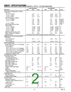
Parameter
Min
150
Max
0.4
Min
150
Max
0.4
Units
OUTPUT STAGE
VOL (IOUT = 10 mA)
IOL
V
VOL<0.8 V
VOL<0.4 V, TMIN–TMAX
15
8
10
250
15
8
10
250
mA
mA
µA
I
OH (Off Leakage)
0.01
200
0.01
200
Delay Time, Positive Clock Edge to
ns
Output Pulse
Fall Time (Load = 500 pF and ISINK = 5 mA)
Output Capacitance
100
5
100
5
ns
pF
OUTPUT ONE-SHOT
Pulsewidth, tOS
COS = 300 pF
COS = 1000 pF
1
4
1.5
5
2
6
1
4
1.5
5
2
6
µs
µs
REFERENCE OUTPUT
Voltage
Drift
4.950
5.0
5.050
100
4.975
5.0
5.025
50
V
ppm/°C
Output Current
Source TMIN to TMAX
Sink
Power Supply Rejection
(Supply Range = 12.5 V to 17.5 V)
Output Impedance (Sourcing Current)
10
100
10
100
mA
µA
500
0.3
500
0.3
0.015
2
0.015
2
%/V
Ω
POWER SUPPLY
Rated Voltage
Operating Range
Dual Supplies
Single Supply (–VS = 0)
Quiescent Current
Digital Common
Analog Common
15
15
11
15
15
11
V
6
+12
18
+36
؎15
+VS – 4
+VS
6
+12
18
+36
؎15
+VS – 4
+VS
V
V
mA
V
V
–VS
–VS
–VS
–VS
TEMPERATURE RANGE
Specified Performance
JP, KP Grade
0
–40
–55
+70
+85
+125
0
–40
+70
+85
°C
°C
°C
AQ, BQ Grade
SQ Grade
NOTES
1Referred to internal VREF. In PLCC package, tested on 10 V input range only.
Specifications in boldface are 100% tested at final test and are used to measure outgoing quality levels.
Specifications subject to change without notice.
ABSOLUTE MAXIMUM RATINGS
DEFINITIONS OF SPECIFICATIONS
GAIN ERROR—The gain of a voltage-to-frequency converter is
that scale factor setting that provides the nominal conversion
relationship, e.g., 1 MHz full scale. The “gain error” is the dif-
ference in slope between the actual and ideal transfer functions
for the V-F converter.
Total Supply Voltage +VS to –VS . . . . . . . . . . . . . . . . . . 36 V
Maximum Input Voltage (Figure 6) . . . . . . . . . . . . . . . . . 36 V
Maximum Output Current (Open Collector Output) . . 50 mA
Amplifier Short Circuit to Ground . . . . . . . . . . . . . Indefinite
Storage Temperature Range: Cerdip . . . . . . –65°C to +150°C
Storage Temperature Range: PLCC . . . . . . –65°C to +150°C
LINEARITY ERROR—The “linearity error” of a V-F is the
deviation of the actual transfer function from a straight line
passing through the endpoints of the transfer function.
GAIN TEMPERATURE COEFFICIENT—The gain tempera-
ture coefficient is the rate of change in full-scale frequency as a
function of the temperature from +25°C to TMIN or TMAX
.
REV. B
–3–

 ADI [ ADI ]