AD652
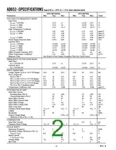
ORDERING GUIDE
Specified
Gain
Drift
Part
ppm/؇C 1 MHz
Temperature Package
Number1 100 kHz Linearity % Range ؇C
Options2
AD652JP
50 max
0.02 max
0.005 max
0.02 max
0.005 max
0.02 max
0 to +70
0 to +70
–40 to +85
–40 to +85
–55 to +125
PLCC (P-20A)
PLCC (P-20A)
Cerdip (Q-16)
Cerdip (Q-16)
Cerdip (Q-16)
AD652KP 25 max
AD652AQ 50 max
AD652BQ 25 max
AD652SQ 50 max
NOTES
1For details on grade and package offerings screened in accordance with MIL-
STD-883, refer to the Analog Devices Military Products Databook or current
AD652/883 data sheet.
2P = Plastic Leaded Chip Carrier; Q = Cerdip.
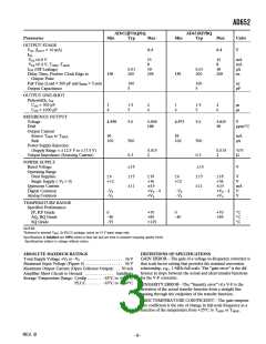
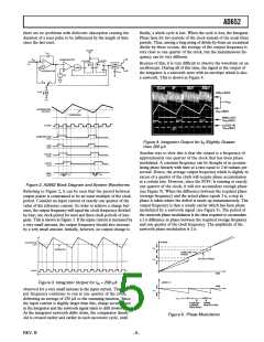
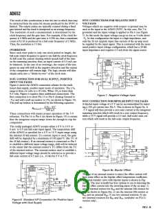
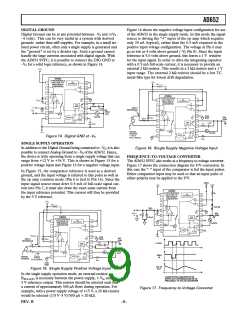
Figure 1a. Cerdip Pin Configuration
PIN CONFIGURATIONS
The pinouts of the AD652 SVFC are shown in Figure 1. A
block diagram of the device configured as a SVFC, along with
various system waveforms, is shown in Figure 2.
PIN
Q-16 PACKAGE
P-20A PACKAGE
1
2
3
+VS
NC
TRIM
TRIM
+VS
NC
4
5
6
7
8
9
10
11
12
13
14
15
16
17
18
19
20
OP AMP OUT
OP AMP “—”
OP AMP “+”
10 VOLT INPUT
–VS
OP AMP OUT
OP AMP “—”
OP AMP “+”
5 VOLT INPUT
10 VOLT INPUT
8 VOLT INPUT
OPTIONAL 10 V INPUT
–VS
COS
CLOCK INPUT
FREQ OUT
DIGITAL GND
ANALOG GND
COMP “—”
COMP “+“
COMP REF
COS
CLOCK INPUT
FREQ OUT
DIGITAL GROUND
ANALOG GND
COMP “—”
COMP “+”
NC
COMP REF
THEORY OF OPERATION
A synchronous VFC is similar to other voltage-to-frequency
converters in that an integrator is used to perform a charge-
balance of the input signal with an internal reference current.
However, rather than using a one-shot as the primary timing
element which requires a high quality and low drift capacitor,
a synchronous voltage-to-frequency converter (SVFC) uses an
external clock; this allows the designer to determine the system
stability and drift based upon the external clock selected. A crys-
tal oscillator may also be used if desired.
Figure 1b. PLCC Pin Configuration
Figure 2 shows the typical up-and-down ramp integrator output
of a charge-balance VFC. After the integrator output has crossed
the comparator threshold and the output of the AND gate has
gone high, nothing happens until a negative edge of the clock
comes along to transfer the information to the output of the
D-FLOP. At this point, the clock level is low, so the latch does
not change state. When the clock returns high, the latch output
goes high and drives the switch to reset the integrator. At the
same time the latch drives the AND gate to a low output state.
On the very next negative edge of the clock the low output state
of the AND gate is transferred to the output of the D-FLOP
and then when the clock returns high, the latch output goes low
and drives the switch back into the Integrate Mode. At the same
time the latch drives the AND gate to a mode where it will truth-
fully relay the information presented to it by the comparator.
The SVFC architecture provides other system advantages besides
low drift. If the output frequency is measured by counting
pulses gated to a signal which is derived from the clock, the
clock stability is unimportant and the device simply performs as a
voltage controlled frequency divider, producing a high resolution
A/D. If a large number of inputs must be monitored simulta-
neously in a system, the controlled timing relationship between
the frequency output pulses and the user supplied clock greatly
simplifies this signal acquisition. Also, if the clock signal is pro-
vided by a VFC, then the output frequency of the SVFC will be
proportional to the product of the two input voltages.
Since the reset pulses applied to the integrator are exactly one
clock period long, the only place where drift can occur is in a
variation of the symmetry of the switching speed with tempera-
ture. Since each reset pulse is identical to every other, the AD652
SVFC produces a very linear voltage to frequency transfer rela-
tion. Also, since all of the reset pulses are gated by the clock,
Hence, multiplication and A-to-D conversion on two signals are
performed simultaneously.
–4–
REV. B

 ADI [ ADI ]