OX9162
OXFORD SEMICONDUCTOR LTD.
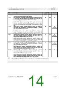
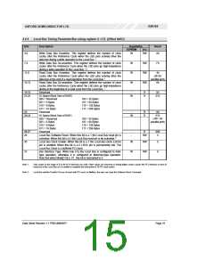
4.4.4 Local Bus Timing Parameter/Bar sizing register 2 ‘LT2’ (Offset 0x0C):
Bits
Description
Read/Write
EEPROM
Reset
PCI
3:0
Write Data Bus Assertion. This register defines the number of clock
cycles after the Reference Cycle when the LBD pins actively drive the
data bus during a write operation to the Local Bus. 1
Write Data Bus De-assertion. This register defines the number of clock
cycles after the Reference Cycle when the LBD pins go high-impedance
during a write operation to the Local Bus. 1,2
Read Data Bus Assertion. This register defines the number of clock
cycles after the Reference Cycle when the LBD pins actively drive the
data bus at the end of a read operation from the Local Bus. 1
Read Data Bus De-assertion. This register defines the number of clock
cycles after the Reference Cycle when the LBD pins go high-impedance
during at the beginning of a read cycle from the Local Bus. 1
Reserved.
W
W
W
W
RW
0h
Fh
7:4
RW
RW
RW
11:8
15:12
4h
(2h for
parallel port)
0h
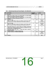
19:16
22:20
-
W
R
R
0h
‘010’
IO Space Block Size of BAR0
000 = Reserved
001 = 4 Bytes
010 = 8 Bytes
011 = 16 Bytes
Reserved
IO Space Block Size of BAR1
000 = Reserved
001 = 4 Bytes
010 = 8 Bytes
011 = 16 Bytes
Reserved
Local Bus Software Reset. When this bit is a 1 the Local Bus reset pin is
activated. When this bit is a 0 the Local Bus reset pin is de-activated. 2
Local Bus Clock Enable. When this bit is a 1 the Local Bus clock (LBCK)
pin is enabled. When this bit is a 0 LBCK pin is permanently low. The
Local Bus Clock is a buffered PCI clock.
Bus Interface Type. When low (=0) the Local Bus is configured to Intel-
type operation, otherwise it is configured to Motorola-type operation.
Note that when Mode[1:0] is ‘01’, this bit is hard wired to 0.
100 = 32 Bytes
101 = 64 Bytes
110 = 128 Bytes
111 = 256 Bytes
23
26:24
-
W
R
R
0h
‘010’
(‘001’ for
parallel port)
100 = 32 Bytes
101 = 64 Bytes
110 = 128 Bytes
111 = 256 Bytes
28:27
29
-
-
R
RW
000
0
30
31
W
W
RW
RW
0
0
Note 1:
Only values in the range of 0 to Ah (0-10 decimal) are valid. Other values are reserved as writing higher values causes the PCI interface to retry all
accesses to the Local Bus as it is unable to complete the transaction in 16 PCI clock cycles.
Note 2:
Local Bus and the Parallel Port are all reset with PCI reset. In Addition, the user can issue the Software Reset Command.
Data Sheet Revision 1.1 PRELIMINARY
Page 15

 OXFORD [ OXFORD SEMICONDUCTOR ]