OX9162
OXFORD SEMICONDUCTOR LTD.
4.3 Accessing logical functions
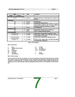
Access to the local bus and parallel port is achieved via standard I/O and memory mapping, at addresses defined by the Base
Address Registers (BARs) in configuration space. The BARs are configured by the system to allocate blocks of I/O and memory
space to the logical function, according to the size required by the function. The addresses allocated can then be used to access
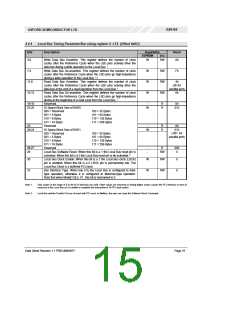
the function. The mapping of these BARs is shown in Table 4.
BAR
Function 0
Local Bus
Parallel Port
0
1
2
3
4
5
CS0 (I/O mapped)
CS1 (I/O mapped)
Local configuration registers (I/O mapped
Local configuration registers (memory mapped)
All CS (memory mapped
Parallel port base registers (I/O mapped)
Parallel port extended registers (I/O mapped)
Unused
Unused
Table 4: Base Address Register definition
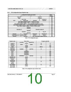
Local Bus
Chip-Select
PCI Offset from BAR 1 in
Function1 (Memory space)
Lower Address Upper Limit
4.3.1 PCI access to 8-bit local bus
When the local bus is enabled (Mode 1), the function
reserves two blocks of I/O space (BAR0 for chip select 0,
BAR1 for chip select 1) and a block of memory space
(BAR4 for chip selects 0 and 1). Each I/O block size is user
definable in the range of 4 to 256 bytes; the memory range
is fixed at 4K bytes.
LBCS0# (LBDS0#)
LBCS1# (LBDS1#)
000h
400h
3FCh
7FCh
Table 5: PCI address map for local bus (memory)
Note: The description given for I/O and memory accesses
is for an Intel-type configuration for the Local Bus. For
Motorola-type configuration, the chip select pins are
redefined to data strobe pins. In this mode the Local Bus
offers up to 8 address lines and two data-strobe pins.
I/O space
In order to minimise the usage of IO space, the block sizes
for BAR0 and BAR1 are user definable in the range of 4 to
256 bytes.
The 8-bit Local Bus has eight address lines (LBA[7:0])
which correspond to the maximum IO address space. If the
maximum allowable block size is allocated to the IO space
(i.e. 256 bytes), then as access in IO space is byte aligned,
LBA[7:0] equal PCI AD[7:0] respectively. When the user
selects an address range which is less than 256 bytes, the
corresponding upper address lines will be set to logic zero.
4.3.2 PCI access to parallel port
When the parallel port is enabled (Mode 0), access to the
port works via BAR definitions as usual with two I/O BARs
corresponding to the two sets of registers defined to
operate an IEEE1284 ECP/EPP and bi-directional Parallel
Port.
The user can change the I/O space block size of BAR0 or
BAR1 as for the local bus mode by over-writing the default
values using the serial EEPROM (see section 4.4).
Memory Space:
The memory base address registers have an allocated
fixed size of 4K bytes in the address space. Since the
Local Bus has 8 address lines and the OX9162 only
implements DWORD aligned accesses in memory space,
the 256 bytes of addressable space per chip select is
expanded to 1K. Unlike an I/O access (where access to
Legacy parallel ports expect the upper register set to be
mapped 0x400 above the base block, therefore if the BARs
are fixed with this relationship, generic parallel port drivers
can be used to operate the device in all modes.
Example: BAR0 = 0x00000379 (8 bytes at address 0x378)
BAR1 = 0x00000779 (8 bytes at address 0x778)
If this relationship is not used, custom drivers will be
needed.
BAR0, BAR1 determines chip-select decoding) for
a
memory access the internal chip-select decoding logic
uses the field PCI AD[10] to decode into 2 chip-select
regions. When the Local Bus is accessed in memory
space, A[9:2] are asserted on LBA[7:0]. The chip-select
regions are defined below.
Data Sheet Revision 1.1 PRELIMINARY
Page 11

 OXFORD [ OXFORD SEMICONDUCTOR ]