OX9162
OXFORD SEMICONDUCTOR LTD.
4.4 Accessing Local configuration registers
The local configuration registers are a set of device specific registers which can always be accessed. They are mapped to the
I/O and memory addresses set up in BAR2 and BAR3, with the offsets defined for each register. I/O or memory accesses can be
byte, word or dword accessed, however on little-endian systems such as Intel 80x86 the byte order will be reversed.
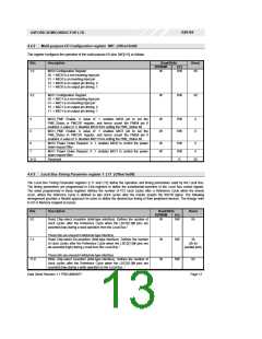
4.4.1 Local Configuration and Control register ‘LCC’ (Offset 0x00)
This register defines control of ancillary functions such as Power Management, endian selection and the serial EEPROM. The
individual bits are described below.
Bits
Description
Read/Write
EEPROM
Reset
PCI
0
2:1
4:3
Mode. This bit returns the state of the Mode pin.
Reserved
Endian Byte-Lane Select for memory access to 8-bit peripherals.
-
R
X
00
00
W
RW
00 = Select Data[7:0]
10 = Select Data[23:16]
01 = Select Data[15:8]
11 = Select Data[31:24]
Memory access to OX9162 is always DWORD aligned. When accessing
8-bit regions this option selects the active byte lane. As both PCI and PC
architectures are little endian, the default value will be used by systems,
however, some non-PC architectures may need to select the byte lane.
Power-down filter time. These bits define a value of an internal filter time
for power-down interrupt request in power management circuitry in
Function0. Once Function0 is ready to go into power down mode,
OX9162 will wait for the specified filter time and if Function0 is still in
power-down request mode, it can assert a PCI interrupt (see section
4.6).
7:5
W
RW
000
000 = power-down request disabled
001 = 4 seconds
010 = 129 seconds
011 = 518 seconds
1XX = Immediate
10:8
Reserved: Power management test bits. The device driver must write
zero to these bits
-
R
000
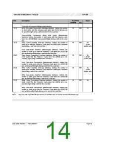
22:11
23
24
Reserved.
-
W
-
R
RW
RW
0000h
0
0
Parallel port Input (glitch) filters. Enabled when ‘1’
EEPROM Clock. For PCI read or write to the EEPROM , toggle this bit to
generate an EEPROM clock (EE_CK pin).
25
26
EEPROM Chip Select. When 1 the EEPROM chip-select pin EE_CS is
activated (high). When 0 EE_CS is de-active (low).
EEPROM Data Out. For writes to the EEPROM, this output bit is the
input-data of the EEPROM. This bit is output on EE_DO and clocked into
the EEPROM by EE_CK.
-
-
RW
RW
0
0
27
EEPROM Data In. For reads from the EEPROM, this input bit is the
output-data of the EEPROM connected to EE_DI pin.
EEPROM Valid. A 1 indicates that a valid EEPROM program is present
Reload configuration from EEPROM. Writing a 1 to this bit re-loads the
configuration from EEPROM. This bit is self-clearing after EEPROM read
Reserved
-
R
X
28
29
-
-
R
RW
X
0
30
31
-
-
R
R
0
0
Reserved
Data Sheet Revision 1.1 PRELIMINARY
Page 12

 OXFORD [ OXFORD SEMICONDUCTOR ]