OX9162
OXFORD SEMICONDUCTOR LTD.
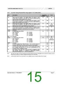
LOCAL BUS
5
provide suitable set up and hold times for common
peripheral devices. However, all the timings can be
increased / decreased independently in multiples of PCI
clock cycles. This feature enables the card designer to
override the length of read or write operations, the address
and chip-select set-up and hold timing, and the data bus
hold timing so that add-in cards can be configured to suit
different speed peripheral devices connected to the Local
Bus. The designer can also program the data bus to
remain in the high impedance state or actively drive the
bus during idle periods.
5.1 Overview
The OX9162 in Mode 1 acts as a bridge from PCI to an 8-
bit Local Bus.
The Local Bus is comprised of a bi-directional 8-bit data
bus, an 8-bit address bus, up to two chip selects, and a
number of control signals that allow for easy interfacing to
standard peripherals. It also provides two active-high or
active-low interrupt inputs (by configuring the MIO pins).
The local bus is configured by LT1 and LT2 (see sections
4.4.3 & 4.4.4) in the Local Configuration Register space. By
programming these registers the card developer can alter
the characteristics of the local bus to suit the
characteristics of the peripheral devices being used.
The local bus will always return to an idle state, where no
chip-select (data-strobe in Motorola mode) signal is active,
between adjacent accesses. During read cycles the local
bus interface latches data from the bus on the rising edge
of the clock where LBRD# (LBDS[1:0]# in Motorola mode)
goes high. Card designers should ensure that their
peripherals provide the OX9162 with the specified data set-
up and hold times with respect to this clock edge.
5.2 Operation
The local bus can be accessed via I/O and memory space.
The mapping to the devices will vary with the application,
but the bus is fully configurable to facilitate simple
development.
The local bus cannot accept burst transfers from the PCI
bus. If a burst transfer is attempted the PCI interface will
signal 'disconnect with data' on the first data phase. The
local bus does accept 'fast back-to-back' transactions from
PCI.
The operation of the local bus is synchronised to the PCI
bus clock. The clock signal is output on pin LBCLK if it has
been enabled by setting LT2[30].
A PCI target must complete the transaction within 16 PCI
clock cycles from assertion of the FRAME# signal,
otherwise it should signal a retry. During a read operation
from the Local Bus, OX9162 waits for master-ready signal
(IRDY#) and computes the number of remaining cycles to
the de-assertion of the read control signal. If the total
number of PCI clock cycles for that frame is greater than
16 clock cycles, OX9162 will post a retry. The master
would normally return immediately and complete the
operation in the following frame.
The eight bit bi-directional pins LBD[7:0] drive the output
data onto the bus during local bus write cycles. For reads,
the device latches the data read from these pins at the end
of the cycle.
The local bus address is placed on pins LBA[7:0] at the
start of each local bus cycle and will remain latched until
the start of the subsequent cycle. If the maximum
allowable block size (256 bytes) is allocated to the local
bus in I/O space, then as access in I/O space is byte
aligned, AD[7:0] are asserted on LBA[7:0]. If a smaller
address range is selected, the corresponding upper
address lines will be set to logic zero.
The control bus is comprised of up to two chip-select
signals LBCS[1:0]#, a read strobe LBRD# and a write
strobe LBWR#, in Intel-type interfaces. For Motorola-type
interfaces, LBWR# is re-defined to perform read/write
control signal (LBRDWR#) and the chip-select signals
(LBCS[1:0]#) are re-defined to data-strobe (LBDS[1:0]#).
A reference cycle is defined, as two PCI clock cycles after
the master asserts the IRDY# signal for the first tstate in
the first cycle after the reference cycle, with offsets to
Data Sheet Revision 1.1 PRELIMINARY
Page 19

 OXFORD [ OXFORD SEMICONDUCTOR ]