OX9162
OXFORD SEMICONDUCTOR LTD.
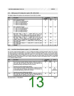
Bits
Description
Read/Write
EEPROM
Reset
PCI
These bits are unused in Motorola-type interface.
15:12
Write Chip-select De-assertion (Intel-type interface). Defines the number
of clock cycles after the reference cycle when the LBCS[1:0]# pins are
de-asserted (high) during a write operation to the Local Bus. 1
W
RW
2h
Read-not-Write De-assertion during write cycles (Motorola-type
interface). Defines the number of clock cycles after the reference cycle
when the LBRDWR# pin is de-asserted (high) during a write to the Local
Bus. 1
19:16
23:20
27:24
31:28
Read Control Assertion (Intel-type interface). Defines the number of
clock cycles after the Reference Cycle when the LBRD# pin is asserted
(low) during a read from the Local Bus. 1
W
W
W
W
RW
RW
RW
RW
0h
(1h for
parallel port)
Read Data-strobe Assertion (Motorola-type interface). Defines the
number of clock cycles after the Reference Cycle when the LBDS[1:0]#
pins are asserted (low) during a read from the Local Bus. 1
Read Control De-assertion (Intel-type interface). Defines the number of
clock cycles after the Reference Cycle when the LBRD# pin is de-
asserted (high) during a read from the Local Bus. 1
3h
(2h for
parallel port)
Read Data-strobe De-assertion (Motorola-type interface). Defines the
number of clock cycles after the Reference Cycle when the LBDS[1:0]#
pins are de-asserted (high) during a read from the Local Bus. 1
Write Control Assertion (Intel-type interface). Defines the number of
clock cycles after the Reference Cycle when the LBWR# pin is asserted
(low) during a write to the Local Bus. 1
0h
(1h for
parallel port)
Write Data-strobe Assertion (Motorola-type interface). Defines the
number of clock cycles after the Reference Cycle when the LBDS[1:0]#
pins are asserted (low) during a write to the Local Bus. 1
Write Control De-assertion (Intel-type interface). Defines the number of
clock cycles after the Reference Cycle when the LBWR# pin is de-
asserted (high) during a write to the Local Bus. 1
2h
Write Data-strobe De-assertion (Motorola-type interface). Defines the
number of clock cycles after the Reference Cycle when the LBDS[1:0]#
pins are de-asserted (high) during a write cycle to the Local Bus. 1
Note 1:
Only values in the range of 0h to Ah (0-10 decimal) are valid. Other values are reserved. See notes in the following page.
Data Sheet Revision 1.1 PRELIMINARY
Page 14

 OXFORD [ OXFORD SEMICONDUCTOR ]